Spacer and preparation method thereof, liquid crystal panel and display device
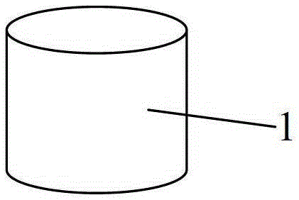
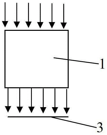
A liquid crystal panel and spacer technology, which is applied in nonlinear optics, instruments, optics, etc., can solve the problems of spacer 1, such as high process requirements, small contact area, local stress concentration, etc., and achieve the elimination of display defects and simple preparation Effect
- Summary
- Abstract
- Description
- Claims
- Application Information
AI Technical Summary
Problems solved by technology
Method used
Image
Examples
Embodiment 1
[0033] image 3 A schematic diagram of the distribution of spacers on the liquid crystal panel in this embodiment is shown, Figure 3a yes image 3 The specific shape diagram of the spacer. Referring to the figure, the spacer 1 of this embodiment is columnar, and the cross-sectional radius of its upper and lower ends is larger than the cross-sectional radius of its middle, so as to realize the contact between the spacer 1 and the upper substrate and the lower substrate 2 in the figure. , the stresses in the contact area are not completely the same, and the schematic diagram of the stress distribution on the cross-section of the spacer is shown in Figure 3b As shown, in the case of the same contact area between the spacer and the substrate in the prior art, the spacer 1 of this embodiment can disperse the stress, forming a Figure 3b The curved stress distribution curve 3 shown in , the spacer 1 with this structure can avoid local stress concentration between the spacer 1 a...
Embodiment 2
[0038] This embodiment provides a method for preparing a spacer, and the specific process can be found in Figure 4 to Figure 9 , the specific description is as follows:
[0039] First, a spacer material layer 4 and a photoresist layer 5 are sequentially formed on the lower substrate 2, see Figure 4 ;
[0040] Next, the photoresist layer 5 is exposed and etched by means of the mask plate 6, and then rinsed with an ultrasonic airflow to form a photoresist pattern 7 corresponding to the spacer distribution position on the photoresist layer 5, See Figure 5 with Image 6 ;
[0041] Then, the spacer material layer 4 is etched by a wet etching process. During the etching process, the concentration gradient of the etchant is realized by adjusting the pressure of the etchant to form a columnar spacer 1, and the upper and lower sides of the spacer 1 The cross-sectional radius at both ends is greater than that in the middle, see Figure 7 with Figure 8 ;
[0042]Wherein, the ...
Embodiment 3
[0045] This embodiment provides a liquid crystal panel, including an upper substrate, a lower substrate, and at least one spacer described in Embodiment 1, the spacer is located between the upper substrate and the lower substrate, and the spacer is The upper end is in contact with the upper substrate, and the lower end of the spacer is in contact with the lower substrate. In the liquid crystal panel formed by using the spacer in Example 1, the stress between the spacer and the upper and lower substrates is dispersed, and local stress concentration is not easy to occur. The phenomenon can improve the display quality of the liquid crystal panel.
PUM
 Abstract
Description
Claims
Application Information


