Mould casting device and method for semiconductor package

A semiconductor and mold-casting technology, which is applied in semiconductor devices, semiconductor/solid-state device manufacturing, semiconductor/solid-state device components, etc., can solve punching, air bubbles and holes, large differences in the properties of sealing plastics, and long sealing process cycles. and other problems, to achieve uniform flow and filling, reduce manufacturing costs, and reduce air holes

Inactive Publication Date: 2013-04-03
SHUNSIN TECH (ZHONG SHAN) LTD
View PDF8 Cites 4 Cited by
  • Summary
  • Abstract
  • Description
  • Claims
  • Application Information

AI Technical Summary

Problems solved by technology

[0003] Since the sealing plastic is injected directly into the mold cavity of the upper mold plate along the runner opening on the edge of the substrate, the mold flow pressure distribution into the mold cavity is relatively uneven, and defects such as punching lines, air bubbles and holes are prone to occur
In addition, due to the long path of the sealing plastic in the mold cavity, the sealing plastic undergoes chemical changes when heated, resulting in a large difference in the properties of the sealing plastic at the front and rear positions in the mold cavity, which affects the sealing quality and requires a longer sealing process cycle.

Method used


Image

  • Mould casting device and method for semiconductor package
  • Mould casting device and method for semiconductor package
  • Mould casting device and method for semiconductor package

Examples


Embodiment Construction

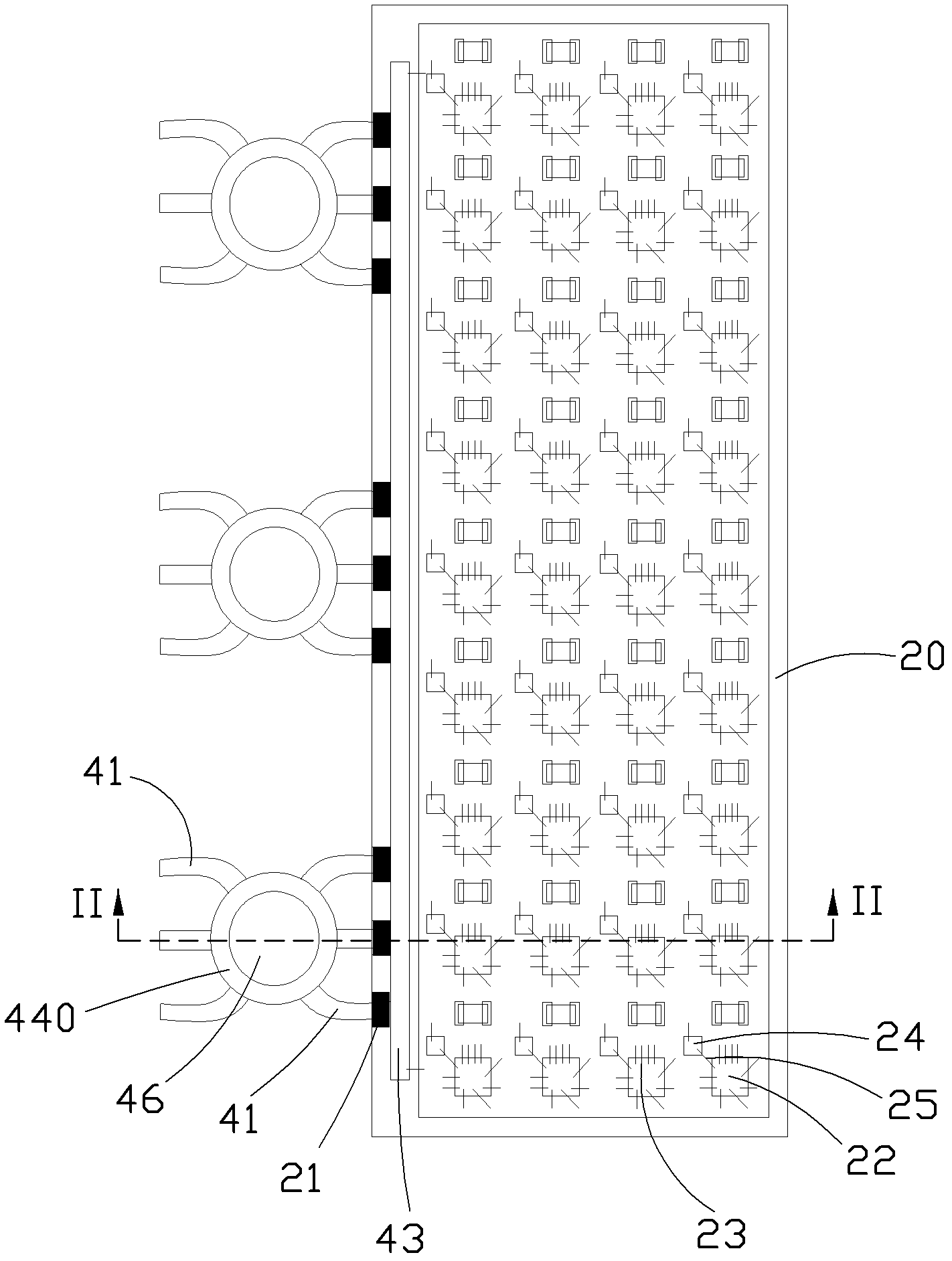
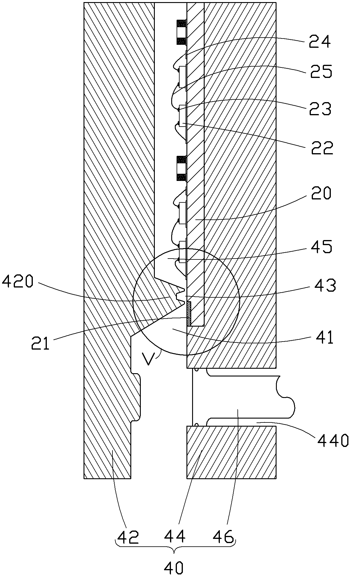
[0053] Please refer to figure 1 with figure 2 , the substrate 20 suitable for packaging, the material of the substrate 20 can be glass epoxy resin (Flame-retardant epoxy-glass fabric composite resin, FR-4, RF-5) or bismaleimide (Bismaleimide Triazine, BT). The substrate 20 is provided with a plurality of chips 22 , a plurality of welding feet 24 and a plurality of welding wires 25 . The chip 22 is provided with a plurality of welding pads 23 , and the welding pads 23 and the welding feet 24 are connected through the bonding wires 25 to electrically connect the chip 22 and the substrate 20 .

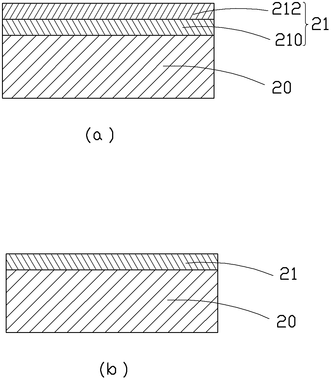
[0054] A debonding layer 21 is disposed on one side of the substrate 20 , and the debonding layer 21 is embedded in the substrate 20 . In this embodiment, the debonding layer 21 is exposed on the surface of the substrate 20 and is coplanar with the surface of the substrate 20 where the chip 22 is located.

[0055] Please refer to image 3 , wherein (a) the debonding layer 21 on the su...


PUM


Abstract

The invention relates to a mould casting device for semiconductor package. The device comprises an upper mould plate, a lower mould plate arranged opposite to the upper mould plate and a piston. The lower mould plate is provided with a plurality of piston ports to accommodate the piston and a pit opened toward the upper mould plate. The pit and the upper mould plate jointly form a mould cavity to accommodate a substrate. The upper mould plate is protruded toward the pit and is adjacent to the protruding part of the piston port. The protruding part close to the lower mould plate is provided with a gap opposite to the pit. An inlet and an outlet communicated with the piston ports and the mould cavity are respectively formed on both sides of the gap, so that a sealing compound injected from the piston ports is injected to the mould cavity along the inlet, the gap and the outlet so as to cover the substrate.

Description

technical field [0001] The invention relates to semiconductor packaging, in particular to a semiconductor packaging molding device and method. Background technique [0002] The existing semiconductor encapsulation molding device includes an upper mold plate with a mold cavity, a lower mold plate with a piston port, a piston, and a substrate accommodated between the upper mold plate and the lower mold plate, and a plurality of chips arranged in an array are arranged on the substrate. A pair of flow channels are arranged on both sides of each piston port to connect with the base plate, and the flow channel openings of the flow channels are connected with the upper template on the base plate. Through the pressure generated by squeezing the piston, the sealing plastic flows from the piston mouth through the runner to the runner mouth and enters the mold cavity of the upper mold plate. After the mold cavity is filled with the molding plastic, the piston remains stationary for a ...

Claims


Application Information

Patent Timeline
IPC IPC(8): H01L21/67H01L21/56B29C45/26
CPCH01L23/3121H01L21/561H01L21/565B29C45/14655B29C45/0046B29C45/02B29C2045/0049H01L2224/32225H01L2224/48137H01L2224/48227H01L2224/73265H01L24/97H01L2224/97H01L2924/181H01L24/73H01L2924/00012H01L2924/00
Inventor 肖俊义
Owner SHUNSIN TECH (ZHONG SHAN) LTD
Why Eureka
Try Eureka