A kind of inas avalanche photodiode and its manufacturing method

An avalanche photoelectric and manufacturing method technology, applied in circuits, electrical components, semiconductor devices, etc., can solve problems such as reducing the maximum gain bandwidth product, inconvenient to apply communication systems, limiting available gain, etc. current, the effect of reducing the tunneling dark current

Inactive Publication Date: 2015-10-21
HUAZHONG UNIV OF SCI & TECH
View PDF3 Cites 0 Cited by
  • Summary
  • Abstract
  • Description
  • Claims
  • Application Information

AI Technical Summary

Problems solved by technology

At present, there are some mainstream methods to reduce the dark current of InAs, such as: 1) low-temperature working method, which enables the APD to work in the range of 290K-77K in a refrigerated environment. Compared with 290K, the dark current at 77K can be reduced by 6 orders of magnitude, but The gain is also reduced from 17 to 8, which reduces the maximum gain-bandwidth product, limits the available gain, and works under cooling, requiring an additional cooling device, which is inconvenient for application in communication systems; 2) Improve the manufacturing process and add a diffusion barrier layer This method reduces the surface dark current and the bulk diffusion current respectively. When the growth temperature of InAs is 470°C, the lattice defects are small. The two-step etching method is adopted. First, the H 3 PO 4 :H 2 o 2 :H 2 O solution followed by 1:8:80 H 2 SO 4 :H 2 o 2 :H 2 O solution, which can reduce the dark current by an order of magnitude, using AlAs 0.16 Sb 0.84 The wide bandgap acts as a minority carrier blocking layer to prevent minority carriers in the p-type contact layer from diffusing to the intrinsic multiplication region, and can also reduce the dark current by an order of magnitude, but the dark current is still high; 3) He ion-implanted planar structure, using ion The method of implantation made InAs APD with flat plate structure to eliminate the surface dark current and increase the resistance of InAs, because the diode is not completely isolated, resulting in a large dark current; 4) Zn diffusion process on semi-insulating substrate, using Zn diffusion method to minimize Surface dark current, using a semi-insulating GaAs substrate, reduces parasitic capacitance, and is easy to integrate with other devices. Zn diffusion can reduce surface dark current, but due to lattice mismatch and defect density, the dark current is still very large; 5) Improve the electric field and Reduce the intrinsic doping concentration method, increase the concentration of the p-type contact layer, thereby increasing the barrier height, reducing the minority carrier diffusion current from the p-type contact layer, and neutralizing the intrinsic Unintentional n-type doping improves the uniformity of the electric field, increases the width of the depletion region, increases the maximum gain, and improves the process to reduce the intrinsic doping concentration, thereby reducing the bulk dark current, and the dark current is reduced by nearly an order of magnitude
The above methods are all improvements for the bulk diffusion dark current and surface leakage current of InAs APD, and the maximum gain is still limited by the tunneling dark current

Method used


Image

  • A kind of inas avalanche photodiode and its manufacturing method
  • A kind of inas avalanche photodiode and its manufacturing method
  • A kind of inas avalanche photodiode and its manufacturing method

Examples


Embodiment 1

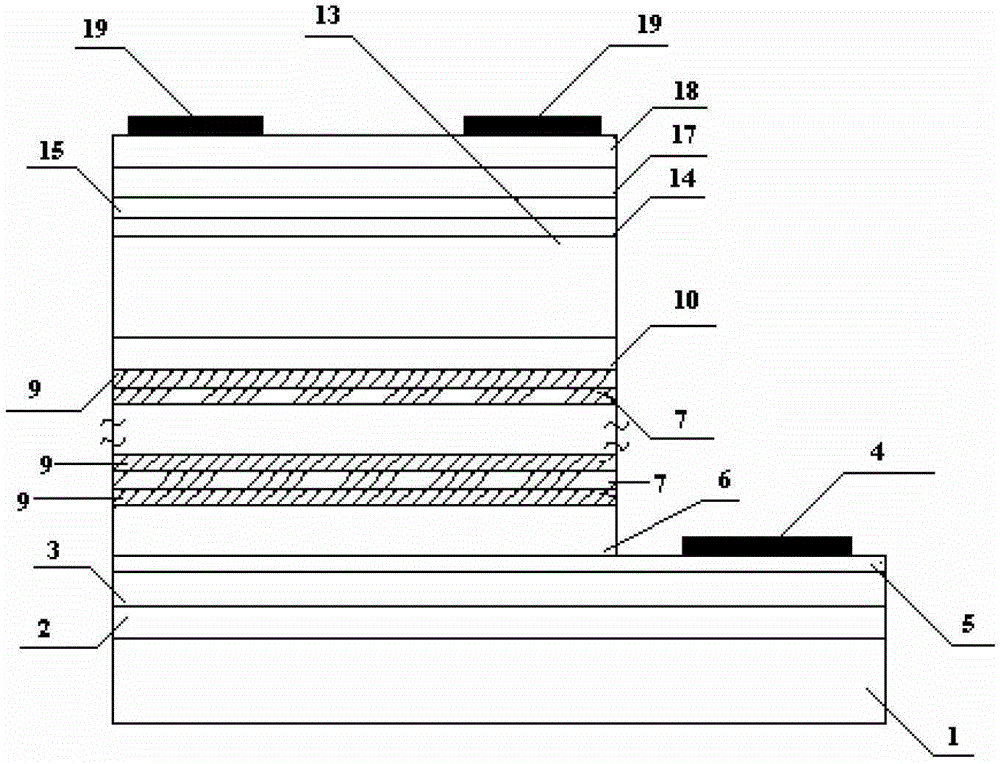
[0042] See figure 1 , When x=0.25, the multiplication layer (7, 9) uses Al 0.25 Ga 0.75 As 0.1052 Sb 0.8948 / InAs superlattice structure; the corresponding charge layer 10 uses Al 0.25 Ga 0.75 As 0.1052 Sb 0.8948 Material, the material of the graded layer is also Al 0.25 Ga 0.75 As 0.1052 Sb 0.8948 It is the same as the charge layer 10 and the multiplication layer 9, so this structure can be omitted. The following provides various structural materials and various parameter tables:

[0043]

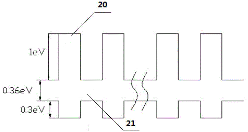
[0044] See Figure 7 , Al 0.25 Ga 0.75 As 0.1052 Sb 0.8948 Schematic diagram of the energy band of / InAs. Adopt Al 0.25 Ga 0.75 As 0.1052 Sb 0.8948 Material as light window layer 17, Al 0.25 Ga 0.75 As 0.1052 Sb 0.8948 The conduction band difference between the material energy band 22 and the InAs material energy band 21 is 0.77 eV, the valence band discontinuity is almost non-existent, and the band gap of the InAs material energy band 21 is 0.36 eV. It is transparent to incident light, can ...

Embodiment 2

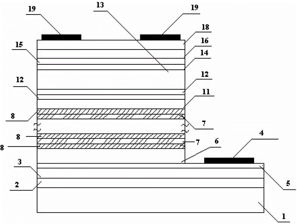
[0048] When x=1, the multiplication layer (7, 8) uses AlAs 0.16 Sb 0.84 / InAs superlattice structure, where the charge layer 11 is AlAs 0.16 Sb 0.84 material.

[0049] A structural material and various parameter tables at this time are given below:

[0050]

[0051]

[0052] This embodiment provides a special case. When x=1, the wide band gap material 8 of the multiplication layer adopts AlAs 0.16 Sb 0.84 . The graded layer 12 is composed of two materials with different compositions.

[0053] See Image 6 , Using AlAs 0.16 Sb 0.84 Material as light window layer 16, AlAs 0.16 Sb 0.84 The conduction band difference between the material energy band 20 and the InAs material energy band 21 is 1eV, the valence band difference is 0.3ev, and the band gap of the InAs material energy band 21 is 0.36ev, which is transparent to incident light and can block a few electrons to the intrinsic region The diffusion reduces the diffusion dark current. Wide band gap materials provide a certain potenti...


PUM


Abstract

The invention relates to an avalanche photodiode and a method for manufacturing the same, in particular to an InAs avalanche photodiode. The photodiode is of an absorbed charge multiplication and separation structure, and multiplication layers are of super-lattice structures. The invention further relates to a method for manufacturing the InAs avalanche photodiode. The method mainly includes steps of S1, generating the multiplication layers of the super-lattice structures with multiple quantum wells; S2, generating charge layers, gradient layers and optical window layers; and S3, forming PN junctions by an Zn diffusion process or a Cd diffusion process. The InAs avalanche photodiode and the method have the advantages that dark current, particularly tunneling dark current, is mainly reduced by the super-lattice structures of the multiplication layers for the narrow-gap attribute of InAs materials; and wide-gap materials matched with the InAs materials are adopted, various structures of the photodiode are further optimized, and accordingly effects of low noise, high gain, high speed and high response are realized.

Description

Technical field [0001] The invention belongs to the technical field of photodiodes, and particularly relates to an InAs avalanche photodiode and a manufacturing method thereof. Background technique [0002] At present, due to the rapid development of optical communication systems, the requirements for the responsiveness and speed of the receiver are getting higher and higher. Compared with PIN detectors, avalanche photodiodes (APDs) have higher sensitivity due to their internal gains and are widely used in optical communication systems. However, the randomness of gain will be accompanied by additional noise; and for traditional APDs such as InAlAs, InP, Si, InGaAs and other materials, there is a limitation of gain-bandwidth product, that is, when the gain is high, the avalanche settling time increases , The bandwidth will be reduced, thus limiting the rate of the receiver. Therefore, the APD with low noise, high response, low dark current, and high gain band-wide product can be...

Claims


Application Information

Patent Timeline
Patent Type & Authority Patents(China)
IPC IPC(8): H01L31/107H01L31/0352H01L31/032H01L31/18
Inventor 赵彦立向静静张冀涂俊杰张诗伯高晶文柯
Owner HUAZHONG UNIV OF SCI & TECH
Why Eureka
Try Eureka