Preparation method of avalanche photodetector

An avalanche photoelectric and detector technology, which is applied in the field of photodetectors, can solve problems such as detector inconsistency, difficulty in Zn diffusion, and reduced yield, so as to achieve reduced tunneling dark current, high crystal quality, and reduced impact The effect of the probability of wearing

Active Publication Date: 2022-01-21
北京英孚瑞半导体科技有限公司
View PDF7 Cites 0 Cited by
  • Summary
  • Abstract
  • Description
  • Claims
  • Application Information

AI Technical Summary

Problems solved by technology

However, Zn diffusion is a difficult and highly variable process to precisely control
Instability of the Zn diffusion process causes detector inconsistencies while reducing yield in production

Method used


Image

  • Preparation method of avalanche photodetector
  • Preparation method of avalanche photodetector
  • Preparation method of avalanche photodetector

Examples


Embodiment 1

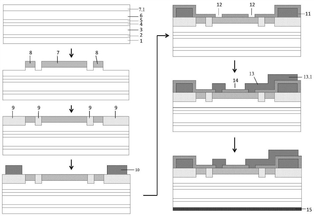
[0051] Such as figure 1 As shown, this implementation case introduces a method for preparing an avalanche photodetector, including the following steps:

[0052] Step 1: On the n-type InP substrate 1, grow n-type InP buffer layer 2, In 0.53 Ga 0.47 As absorption layer 3, In x Ga 1-x As y P 1-y Bandwidth gradient layer 4, n-type InP charge control layer 5, intrinsic InP multiplication layer 6, p-type InP capping layer 7.1.

[0053] Step 2: Using SiO 2 Patterning the hard mask, using an etching method to etch the p-type InP capping layer 7 and part of the intrinsic type InP multiplication layer 6 in a specific area, the thickness of the p-type InP capping layer 7.1 is 1um, and the thickness of the intrinsic InP multiplication layer 6 It is 500nm, and the etching depth is 1.2um, that is, the 1.2um etching depth includes the 1um thick p-type InP capping layer and the 0.2um deep intrinsic InP multiplication layer under the p-type InP capping layer, and the remaining InP cappi...

Embodiment 2

[0060] On the basis of the first embodiment, further, the n-type InP substrate 1 is heavily doped and forms an ohmic contact with the back electrode 15 . The n-type InP buffer layer 2 has a thickness of 0.5um, and its function is to better match the n-type InP substrate 1 and In 0.53 Ga 0.47 The difference in lattice constant between the As absorption layers 3 due to different growth conditions ensures the growth quality of the epitaxial layer.

[0061] The In 0.53 Ga 0.47 The thickness of the As absorption layer 3 is 2um, and the background doping concentration is less than 1×10 15 / cm 3 , this layer is a photogenerated carrier generation layer, designed to absorb photon energy with a wavelength of 1.0-1.7um as much as possible.

[0062] The In x Ga 1-x As y P 1-y The bandwidth gradient layer 4 consists of three layers, and the bandwidths of each layer are 0.95eV, 1.03eV and 1.13eV from bottom to top; the three-layer bandwidth gradient layer starts from In 0.53 Ga ...


PUM

PropertyMeasurementUnit
thicknessaaaaaaaaaa
thicknessaaaaaaaaaa
thicknessaaaaaaaaaa

Abstract

The invention discloses a preparation method of an avalanche photodetector. An n-type InP buffer layer, an In0.53Ga0.47As absorption layer, an InxGa1-xAsyP1-y bandwidth gradient layer, an n-type InP charge control layer, an intrinsic InP multiplication layer and a p-type InP cover layer are sequentially grown on an n-type InP substrate; then the cover layer and a part of the multiplication layer are corroded, a central collector region and an electric field protection ring surrounding the central collector region are formed in the residual cover layer region after corrosion, and then an InP barrier layer is generated in the corroded region through secondary epitaxy; then a SiO2 layer is deposited, and SiO2 in a partial region is etched off to form a circle of annular SiO2 isolation layer on the InP isolation layer; an optical anti-reflection film is deposited and a metal contact window is formed on the optical anti-reflection film above the central collector region; then an upper electrode is constructed, wherein the upper electrode is in contact with the central collector region through the metal contact window; and finally, a back electrode is prepared on the back surface of the InP substrate.

Description

technical field [0001] The invention belongs to the technical field of photodetectors, and in particular relates to a preparation method of an avalanche photodetector. Background technique [0002] The working principle of the avalanche photodetector is to use the p-i-n junction under a relatively high reverse bias electric field. Photons are incident on the i region to make electrons transition from the valence band to the conduction band, forming electron-hole pairs. Under the action of a strong electric field, the electrons- The hole pairs get accelerated, collide with other atoms, create additional electron-hole pairs and keep on happening. Since the incidence of fewer photons or even a single photon can trigger the avalanche multiplication process and cause changes in the macroscopic current, the avalanche photodetector has extremely high sensitivity and detection efficiency, and has a very high potential in the field of weak light detection or even single photon detect...

Claims


Application Information

Patent Timeline
Patent Type & Authority Applications(China)
IPC IPC(8): H01L31/18H01L31/107
CPCH01L31/1844H01L31/1075Y02P70/50
Inventor 杨志茂王斌
Owner 北京英孚瑞半导体科技有限公司
Why Eureka
Try Eureka