On-chip heating type germanium photoelectric detector for 2-micron wave band

A photodetector and heating technology, applied in the field of photodetectors, can solve problems such as low responsivity and poor integration, achieve high responsivity, balance between responsivity and bandwidth performance, and reduce tunneling dark current

Pending Publication Date: 2022-08-05
HARBIN INST OF TECH SHENZHEN GRADUATE SCHOOL
View PDF0 Cites 0 Cited by
  • Summary
  • Abstract
  • Description
  • Claims
  • Application Information

AI Technical Summary

Problems solved by technology

[0004] Aiming at the above technical problems, the present invention discloses an on-chip heating germanium photodetector for 2 micron band, which solves the problems of poor integration and low responsivity of the existing 2 micron communication band on-chip photodetector. The device has a compact structure, Advantages of high responsiveness, compatibility with silicon-based CMOS process, and compatibility with conventional MPW tape-out process

Method used


Image

  • On-chip heating type germanium photoelectric detector for 2-micron wave band
  • On-chip heating type germanium photoelectric detector for 2-micron wave band
  • On-chip heating type germanium photoelectric detector for 2-micron wave band

Examples


Embodiment Construction

[0036] The preferred embodiments of the present invention will be further described in detail below.

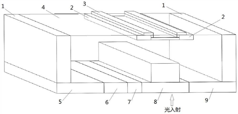
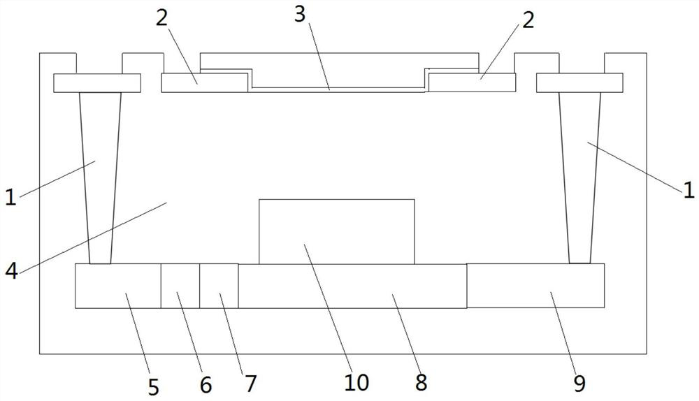
[0037] like figure 1 and figure 2 As shown in the figure, an on-chip heated germanium photodetector for 2 μm waveband adopts a lateral PN junction structure. The detector includes: two aluminum electrodes 1, two TiN heating electrodes 2, a TiN heating layer 3, and N heavy doping The structure of the heterosilicon layer 5 , the P heavily doped silicon layer 9 , the germanium absorption layer 10 , the silicon intrinsic layer 8 , the silicon multiplication layer 6 , and the P lightly doped silicon charge layer 7 .

[0038]The N heavily doped silicon layer 5 and the P heavily doped silicon layer 9 are located on both sides, and the tops thereof are respectively connected to two aluminum electrodes, the silicon multiplication layer 6, the P lightly doped silicon charge layer 7, the The intrinsic layers 8 are connected in sequence and laterally located between the N heavily dope...


PUM

PropertyMeasurementUnit
widthaaaaaaaaaa
widthaaaaaaaaaa
widthaaaaaaaaaa

Abstract

The invention provides an on-chip heating type germanium photoelectric detector for a 2-micron wave band. The on-chip heating type germanium photoelectric detector comprises two electrodes, two TiN heating electrodes, a TiN heating layer, an N heavily-doped silicon layer, a P heavily-doped silicon layer, a germanium absorption layer, a silicon intrinsic layer, a silicon multiplication layer and a P lightly-doped silicon charge layer, the N heavily-doped silicon layer and the P heavily-doped silicon layer are located on the two sides and connected with the two electrodes respectively, the silicon multiplication layer, the P lightly-doped silicon charge layer and the silicon intrinsic layer are sequentially located between the N heavily-doped silicon layer and the P heavily-doped silicon layer, the germanium absorption layer is arranged above the silicon intrinsic layer and connected with the silicon intrinsic layer, the TiN heating layer is located above the germanium absorption layer, and the N heavily-doped silicon layer and the P lightly-doped silicon charge layer are connected with the silicon intrinsic layer. The germanium absorption layer is isolated from the TiN heating layer and the TiN heating electrode through fillers. According to the technical scheme, the device is compact in structure, high in responsivity and compatible with the silicon-based CMOS technology.

Description

technical field [0001] The invention relates to the technical field of photodetectors, in particular to an on-chip heating germanium photodetector for 2-micron waveband. Background technique [0002] With the continuous development of modern communication technology, people's requirements for high-speed, high-bandwidth and low-latency communication links are getting higher and higher. For the development of optical communication, it is very important to break through the communication capacity limitations brought by traditional communication bands. . At present, the wavelength channel of the traditional C-band wavelength division multiplexing has been saturated, and the thulium-doped fiber has a gain spectrum width of 1700nm-2100nm, which can provide broadband optical amplification, while the C-band erbium-doped fiber does not have such a wide gain spectrum, and 2μm The fiber loss in the band can be the same as that of standard single-mode fiber. Extending the communicatio...

Claims


Application Information

Patent Timeline
Patent Type & Authority Applications(China)
IPC IPC(8): H01L31/105H01L31/0216H01L31/024
CPCH01L31/024H01L31/02161H01L31/105Y02P70/50
Inventor 徐科王嘉宁
Owner HARBIN INST OF TECH SHENZHEN GRADUATE SCHOOL
Why Eureka
Try Eureka