
Method for preparing semiconductor sub-micron band on flexible substrate, and flexible optical waveguide

A flexible substrate and semiconductor technology, applied in the field of flexible optical waveguides, can solve the problems of film surface tension damage, agglomeration into clusters, disordered ordering, etc.

Active Publication Date: 2015-07-01
SHANGHAI INST OF MICROSYSTEM & INFORMATION TECH CHINESE ACAD OF SCI +1
View PDF5 Cites 2 Cited by
  • Summary
  • Abstract
  • Description
  • Claims
  • Application Information

AI Technical Summary

Problems solved by technology

The small-sized nano-film has insufficient attraction to the silicon substrate, which causes the film to be disordered or even clustered due to the destruction of the surface tension of the solution during the process of etching away the buried oxide layer and taking it out of the solution.

Method used


Image

  • Method for preparing semiconductor sub-micron band on flexible substrate, and flexible optical waveguide
  • Method for preparing semiconductor sub-micron band on flexible substrate, and flexible optical waveguide
  • Method for preparing semiconductor sub-micron band on flexible substrate, and flexible optical waveguide

Examples


Embodiment 1

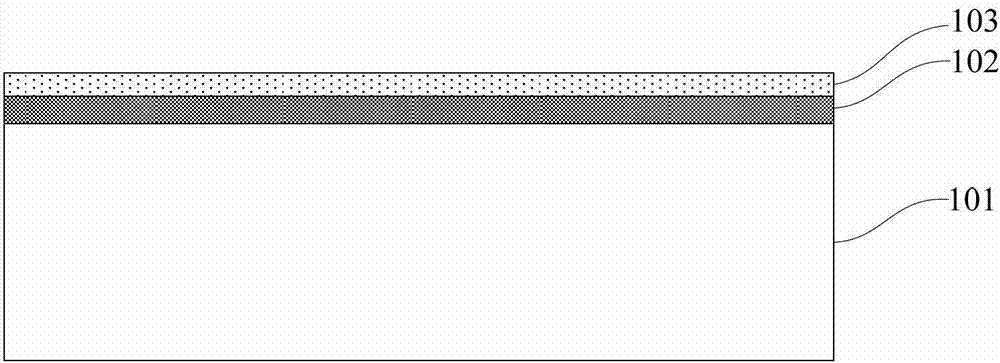
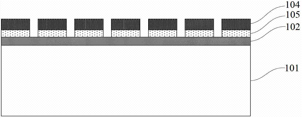
[0039] Such as Figure 1~Figure 8b As shown, this embodiment provides a method for preparing a semiconductor sub-micron belt on a flexible substrate based on an edge transfer method, which at least includes the following steps:

[0040] Such as Figure 1~Figure 2 As shown, step 1) is first performed to provide a semiconductor-on-insulator substrate including a silicon substrate 101, a buried oxide layer 102, and a top semiconductor 103, and a plurality of strips are formed on the surface of the top semiconductor 103 in a photolithography 胶图104。 Glue graphics 104.

[0041] In this embodiment, the semiconductor-on-insulator substrate is an SOI substrate, and the top-layer semiconductor 103 can be used to transfer a microbelt structure of any material to a flexible substrate according to material requirements in actual applications, such as Germanium, three-five group compound semiconductor materials, etc.

[0042] Specifically, a semiconductor-on-insulator substrate including a silico...

Embodiment 2

[0055] Such as Figure 1~Figure 8b As shown, this embodiment provides a flexible optical waveguide prepared based on the edge transfer method, when the semiconductor-on-insulator substrate is an SOI substrate, that is, the top semiconductor is silicon, and the strips are rectangular strips. The semiconductor sub-micron tape on the flexible substrate prepared by the method for preparing the semiconductor sub-micron tape on the flexible substrate based on the edge transfer method described in Example 1 can be directly used as a flexible optical waveguide material, so the basic steps are as in the example 1. Of course, it is also possible to obtain a flexible optical waveguide with required functions by performing certain processing on the semiconductor sub-micron strip on the flexible substrate.

[0056] In summary, the present invention provides a method for preparing semiconductor submicron bands on a flexible substrate based on the edge transfer method and a flexible optical wave...


PUM

PropertyMeasurementUnit
widthaaaaaaaaaa
widthaaaaaaaaaa

Abstract

The invention relates to a method for preparing a semiconductor sub-micron band on a flexible substrate, and a flexible optical waveguide. The method is based on an edge transfer method. According to the method, top-layer semiconductor on a semiconductor substrate on an insulator is etched into alternately arranged semiconductor strip structures; a buried oxide layer is corroded into a plurality of supporting structures by using an HF solution, such that suspended semiconductor band structures are formed on two sides of each semiconductor strip structure; a PDMS substrate is subjected to conformal contact with the semiconductor strip structures; the PDMS substrate is lifted towards a preset direction, such that the semiconductor band structures are separated from the semiconductor strip structures and are transferred to the PDMS substrate; and a silicon optical waveguide on the flexible substrate can be prepared with the prepared semiconductor sub-micron band. For a first time, the invention provides the method for realizing the transferring of the semiconductor sub-micron band to the flexible substrate by controlling the corrosion of the edges of the semiconductor material on the insulator. The controllability of the width and arrangement of the semiconductor sub-micron band are high. The semiconductor sub-micron band can be used for manufacturing devices with relatively high precisions. The method is simple, effective, and has low cost.

Description

Technical field [0001] The invention relates to a semiconductor structure and a preparation method, in particular to a method for preparing a semiconductor submicron band on a flexible substrate based on an edge transfer method and a flexible optical waveguide. Background technique [0002] In 1965, Gordon Moore pointed out: "As transistor sizes decrease, the number of transistors on silicon microprocessors will double every 18-24 months." This statement has been developed into the well-known Moore's Law, which is also regarded by the industry as the driving force for the development of the entire microelectronics industry, which has made the integration of integrated circuits and devices increasingly smaller. After 40 years of development of modern microelectronics technology, macroelectronics technology began to appear, and it has sprung up rapidly, occupying a considerable share of the market. Because the required coverage area in macroelectronics technology is much larger th...

Claims


Application Information

Patent Timeline
Patent Type & Authority Patents(China)
IPC IPC(8): B81C1/00G02B6/122G02B6/13
Inventor 狄增峰郭庆磊梅永丰张苗黄高山郑晓虎
Owner SHANGHAI INST OF MICROSYSTEM & INFORMATION TECH CHINESE ACAD OF SCI
Learn More