
Graphene nanoribbons Fin-FET (Field Effect Transistor) device with controllable channel width and preparation method thereof

A graphene nanoribbon and channel width technology, applied in semiconductor/solid-state device manufacturing, semiconductor devices, electrical components, etc., can solve the problems of high cost, low yield, time-consuming, etc., to avoid direct contact, and the method is simple , Easy to remove glue effect

Inactive Publication Date: 2014-01-08
FUDAN UNIV
View PDF3 Cites 5 Cited by
  • Summary
  • Abstract
  • Description
  • Claims
  • Application Information

AI Technical Summary

Problems solved by technology

To prepare graphene nanoribbon Fin-FET devices with narrow channel width, traditional methods include electron beam lithography and scanning tunneling microscope (STM) lithography, but there are many shortcomings such as time-consuming, expensive, and low yield.
At present, relatively novel methods include centrifugal exfoliation, plasma etching, and using silicon nanowires as etching masks, etc., but it is still a huge challenge to realize large-area preparation of graphene nanomaterials with controllable size.

Method used


Image

  • Graphene nanoribbons Fin-FET (Field Effect Transistor) device with controllable channel width and preparation method thereof
  • Graphene nanoribbons Fin-FET (Field Effect Transistor) device with controllable channel width and preparation method thereof
  • Graphene nanoribbons Fin-FET (Field Effect Transistor) device with controllable channel width and preparation method thereof

Examples


Embodiment Construction

[0027] An exemplary embodiment of the present invention will be described in detail below with reference to the accompanying drawings. In the drawings, for convenience of description, the thicknesses of layers and regions are enlarged or reduced, and the shown sizes do not represent actual sizes. The representations in the referenced figures are schematic, but this should not be considered as limiting the scope of the invention. Also in the following description, the term substrate used may be understood to include the substrate being processed, possibly including other thin film layers prepared thereon.

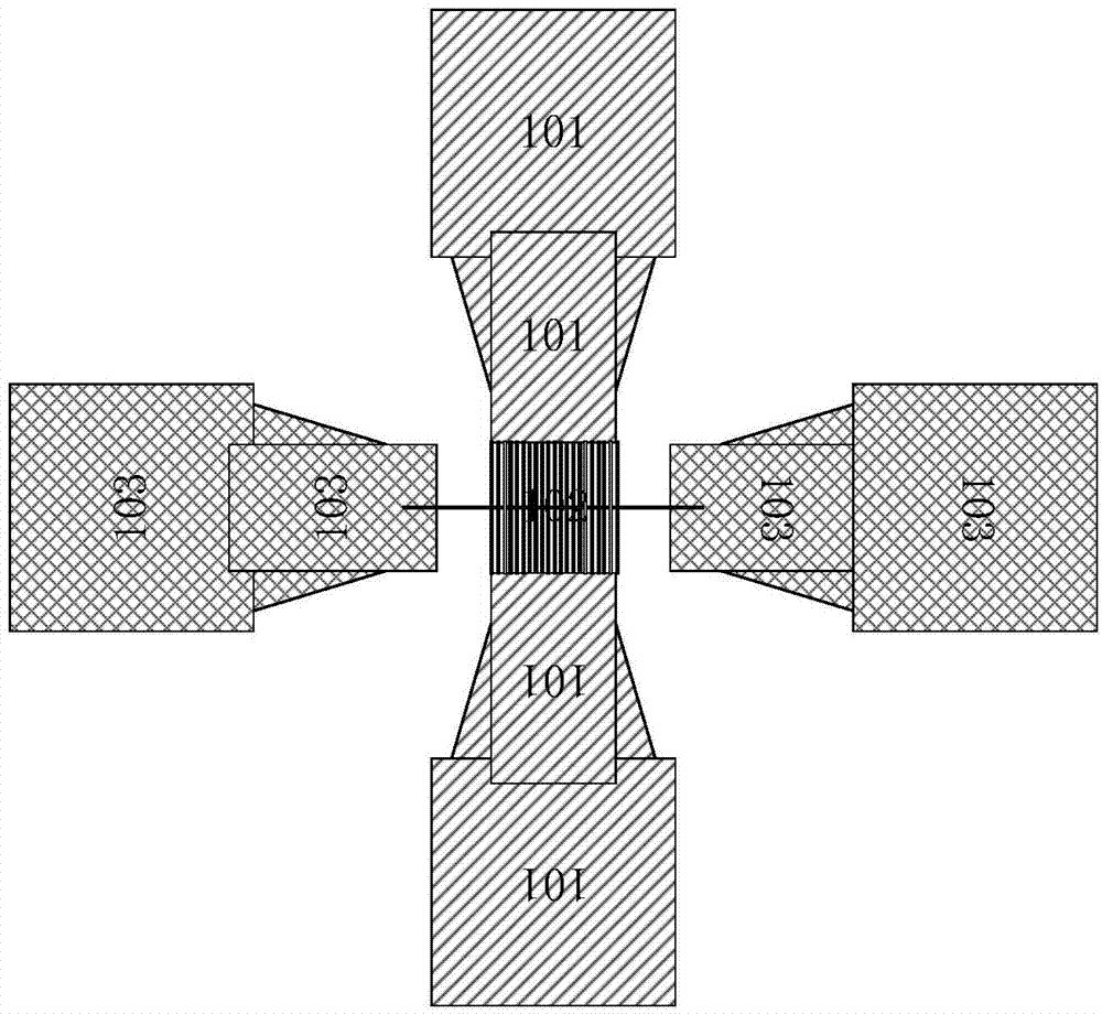
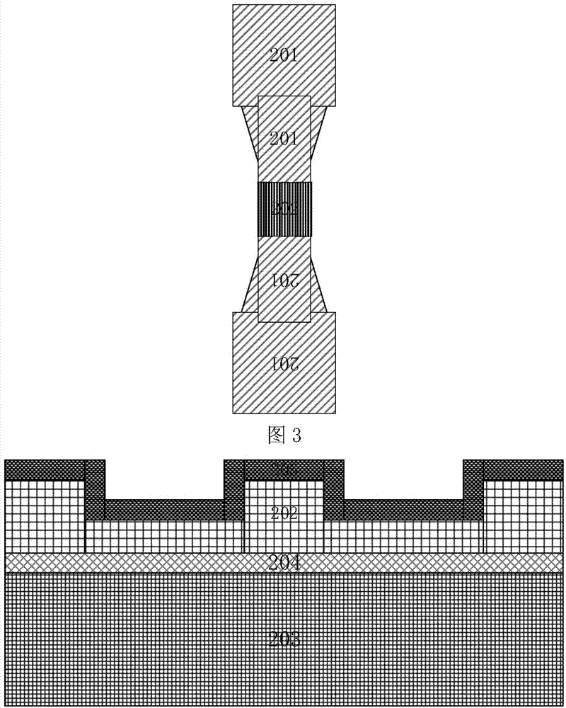
[0028] figure 1 It is a cross-sectional view of an example of a graphene nanoribbon Fin-FET device unit with controllable channel width. like Figure 2-Figure 8 As shown, Ti / Au is selected for the source / drain electrode 201, PVA is selected for the resist 202, located on the silicon / silicon dioxide substrate 203 and the transferred single-layer graphene 204, and Ti / Au is...


PUM

PropertyMeasurementUnit
thicknessaaaaaaaaaa

Abstract

The invention belongs to the technical field of graphene nanometer devices, and particularly relates to a graphene nanoribbons Fin-FET (Field Effect Transistor) device with controllable channel width and a preparation method thereof. The preparation method is suitable for preparing the graphene nanoribbons Fin-FET device on a large scale, and comprises the following steps of: firstly preparing a registration mark and a source / drain electrode of the Fin-FET device on grapheme by utilizing a general electron beam lithography method; then sequentially preparing a grapheme island and a hundred-nanoscale photoresist line pattern on a grapheme sample by utilizing an electron beam registration method; depositing a side wall through an atomic layer, and realizing accurate control on the width of the side wall; and etching by adopting the side wall as a mask through side wall transfer technology, so that the accurate control on the channel width of the graphene nanoribbons is realized. Through adjusting the periodicity of atomic layer deposition, a graphene nanoribbons Fin-FET device array with the channel width being less than 10nm can be prepared on a large scale.

Description

technical field [0001] The invention belongs to the technical field of graphene nano-devices, in particular to a graphene nano-ribbon Fin-FET device with controllable channel width and a preparation method thereof. Background technique [0002] As the size of semiconductor devices is further scaled down, traditional silicon-based devices will reach their size limit. The semiconductor industry has conducted a series of research and exploration on materials and processes suitable for device miniaturization. Among them, graphene has attracted extensive attention from researchers in the industry due to its excellent mechanical strength and Young's modulus, very high electrical and thermal conductivity, and inherent high mobility characteristics. [0003] Graphene is a two-dimensional material with zero band gap, and as early as 2006, Y.-W. Son proposed the theory of introducing a band gap to graphene by making extremely narrow graphene. P. Kim et al. verified through experimen...

Claims


Application Information

Patent Timeline
Patent Type & Authority Applications(China)
IPC IPC(8): H01L29/78H01L29/10H01L21/336
CPCH01L29/1033H01L29/66484H01L29/7831
Inventor 孙清清戴亚伟王鹏飞张卫周鹏
Owner FUDAN UNIV
Learn More