Nano-diamond coating package substrate

A technology of nano-diamond and packaging substrate, which is applied in the direction of electrical components, electrical solid devices, circuits, etc., and can solve problems such as low thermal resistance

Inactive Publication Date: 2013-05-01
DONGGUAN SINOINNOVO SEMICON LIGHTING
View PDF5 Cites 1 Cited by
  • Summary
  • Abstract
  • Description
  • Claims
  • Application Information

AI Technical Summary

Problems solved by technology

[0004] The purpose of the present invention is to solve the deficiencies in the prior art, provide a nano-diamond coating packaging substrate with high thermal conduct

Method used


Image

  • Nano-diamond coating package substrate
  • Nano-diamond coating package substrate
  • Nano-diamond coating package substrate

Examples


Embodiment Construction

[0015] In order to further understand the features, technical means, and achieved specific objectives and functions of the present invention, and to analyze the advantages and spirit of the present invention, the present invention will be further described through the following examples.

[0016] The development of the LED industry is also focused on high-power, high-brightness, and small-size LED products. Therefore, providing heat-dissipating substrates with high heat dissipation, precise dimensions, and no thermal distortion will also become the development of LED heat-dissipating substrates in the future. trend.

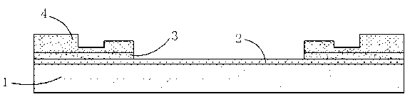
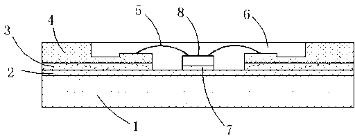
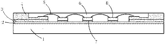
[0017] Such as Figures 1 to 3 As shown, the present invention uses a graphite sheet 1 as a carrier, and a nano-diamond coating layer 2 is introduced into the surface of the graphite sheet 1, and the surface of the graphite sheet 1 is coated with a nano-diamond coating layer 2 by a nano-diamond coating process, and the nano-diamond coating layer 2 is nanoscale S...


PUM

PropertyMeasurementUnit
Thicknessaaaaaaaaaa
Surface hardnessaaaaaaaaaa

Abstract

The invention discloses a nano-diamond coating package substrate, which is high in heat conductivity, low in heat resistance, high in reliability, low in cost, improved in LED (Light Emitting Diode) light-emitting efficiency and prolonged in service life. According to the nano-diamond coating package substrate, a graphite flake is used as a carrier, a nano-diamond coating layer is introduced onto the surface of the graphite flake, organic silica gel is arranged on the upper surface of the nano-diamond coating layer, the organic silica gel is distributed at two sides of the nano-diamond coating layer, a conductive welding plate is arranged on the organic silica gel, one or more LED chips are arranged on the nano-diamond coating layer, the LED chips are positioned between conductive welding plates at two sides, the LED chips are connected with the conductive welding plates through interconnecting wires, and the LED chips are adhered on the nano-diamond coating layer through chip heat-conduction gel. The nano-diamond coating package substrate disclosed by the invention has the advantages of enhancing the hardness of a package surface by carrying out a nano-diamond coating process on the package surface, enhancing the light reflectivity and being good in heat dissipation effect.

Description

technical field [0001] The invention relates to an LED packaging substrate, in particular to a nano-diamond coating substrate for high-power LED chip packaging. Background technique [0002] The LED heat dissipation substrate mainly utilizes the good thermal conductivity of the heat dissipation substrate material itself to guide the heat source from the LED grain. Therefore, from the description of the LED heat dissipation method, we can divide the LED heat dissipation substrate into two categories, namely (1) LED chip substrate and (2) system circuit board. These two different heat dissipation substrates carry LEDs respectively. The heat generated by the die and the LED chip when the LED die emits light passes through the heat dissipation substrate of the LED die to the system circuit board, and then is absorbed by the atmospheric environment to achieve the effect of heat dissipation. [0003] To improve LED luminous efficiency and service life, solving the heat dissipati...

Claims


Application Information

Patent Timeline
IPC IPC(8): H01L33/64H01L33/60
CPCH01L2224/48091H01L2224/48137H01L2224/73265H01L2924/00014
Inventor 赵利民
Owner DONGGUAN SINOINNOVO SEMICON LIGHTING
Why Eureka
Try Eureka