

ROM (Read Only Memory) and layout thereof
A memory and layout technology, applied in the field of integrated circuits, can solve the problems of large unit information storage area and shrinkage of ROM basic storage units, and achieve the effect of reducing the storage area
- Summary
- Abstract
- Description
- Claims
- Application Information
AI Technical Summary
Problems solved by technology
Method used
Image

Examples
Embodiment 1
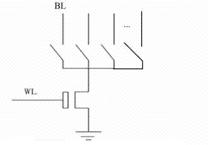
[0033] This embodiment provides a ROM memory, including: at least one MOS transistor, a bit line and a word line, wherein, as figure 1 As shown, the drain of each MOS transistor corresponds to at least two bit lines BL, the gate of the MOS transistor is connected to the word line WL, and the source of the MOS transistor is grounded.
[0034] The connection states of two or more bit lines and MOS transistors can make the MOS transistors store more than two kinds of state information. That is, under the premise of a certain ROM memory area, by increasing the number of bit line regions, the programmable information of one MOS transistor of the ROM memory can be greater than 1 bit, and the storage area of 1 bit information is correspondingly reduced.
Embodiment 2
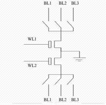
[0036] This embodiment discloses a ROM memory layout corresponding to the above embodiments, including at least one MOS tube area, a word line area and a bit line area.
[0037] Among them, such as figure 2 As shown, the MOS tube region source region S, source metal region SM, drain region D, drain metal region DM, gate region G and gate metal region GM. The source metal region SM, the drain metal region DM and the gate metal region GM all extend along a first direction and are arranged along a second direction, and the first direction is perpendicular to the second direction. And the source metal region SM is located in the source region S, the drain metal region DM is located in the drain region D, and the gate metal region GM is located in the gate region G, between the source metal region SM and the source region S Contact holes are provided between the drain metal region DM and the drain region D, and between the gate metal region GM and the gate region G, so as to real...
Embodiment 3
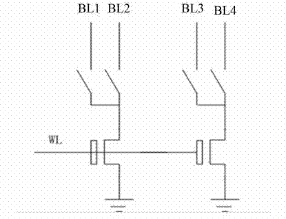
[0044] This embodiment discloses another ROM memory, which includes a MOS transistor, a word line and three bit lines.
[0045] Such as image 3 As shown, the source of the MOS transistor is grounded, the gate is connected to the word line WL, and the drain corresponds to three bit lines, namely the first bit line BL1, the second bit line BL2 and the third bit line BL3.
[0046] Among them, only one of the first bit line BL1, the second bit line BL2 and the third bit line BL3 can be connected to the drain of the MOS transistor at most. When the third bit line BL3 is connected to the drain, a MOS transistor stores The state information of the MOS transistor is "00"; when the second bit line BL2 is connected to the drain, the state information stored in a MOS transistor is "01"; when the first bit line BL1 is connected to the drain, a MOS transistor The stored status information is "10"; when no bit line is connected to the drain, the stored status information of a MOS transist...
PUM
 Abstract
Description
Claims
Application Information