Sealing system

A packaging system and unified technology, applied in the direction of semiconductor/solid-state device components, semiconductor devices, electrical components, etc., can solve the problems of increasing system volume, electromagnetic interference can not be shielded, etc., to improve sensitivity, solve EMC problems, and shield interference Effect

Active Publication Date: 2013-05-08
NAT CENT FOR ADVANCED PACKAGING
View PDF7 Cites 22 Cited by
  • Summary
  • Abstract
  • Description
  • Claims
  • Application Information

AI Technical Summary

Problems solved by technology

However, the metal frame can only play the role of shielding the interference of the external magnetic field to the internal components of the system and other sensitive sources of external radiation interference of the internal components of the system, ...

Method used


Image

  • Sealing system
  • Sealing system
  • Sealing system

Examples


Embodiment 1

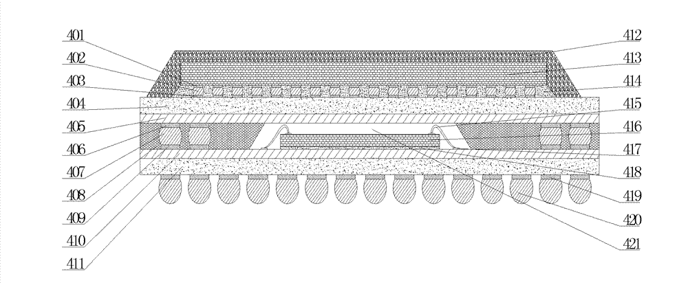
[0044] refer to figure 1 , figure 1 The packaging system shown in the figure includes: an upper substrate 404 and a lower substrate 411 that are arranged oppositely. In this embodiment, the upper substrate 404 and the lower substrate 411 are two independent rigid substrates; the side of the lower substrate 411 facing the upper substrate 404 is provided with The lower shielding layer 410, the upper shielding layer 405 is arranged on the side of the upper substrate 404 facing the lower substrate 411, the lower shielding layer 410 and the upper shielding layer 405 can be grounded or connected to a power supply (not shown in the figure), if connected to the power supply, it can The power supply for the packaging system is connected. In this embodiment, the upper shielding layer 405 and the lower shielding layer 410 are two mutually independent shielding layers. The materials of the upper shielding layer 405 and the lower shielding layer 410 can be copper, aluminum and other metal...

Embodiment 2

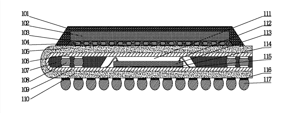
[0052] The difference from Embodiment 1 is that in the packaging system described in this embodiment, the substrate in it is a flexible substrate, and the flexible substrate is bent into a U-shaped substrate. For details, please refer to figure 2 .

[0053] The packaging system includes: a U-shaped substrate formed by folding the same flexible substrate in half, the U-shaped substrate includes an opposite upper substrate 105 and a lower substrate 110; the inner wall of the U-shaped substrate is provided with a U-shaped shielding layer, the The U-shaped shielding layer completely covers the inner wall of the U-shaped substrate, and the U-shaped shielding layer includes an upper shielding layer 106 and a lower shielding layer 109 opposite to each other. The U-shaped shielding layer is grounded or connected to a power supply (not shown in the figure), The material of the U-shaped shielding layer is similar to the material of the shielding layer described in Embodiment 1, and wil...

Embodiment 3

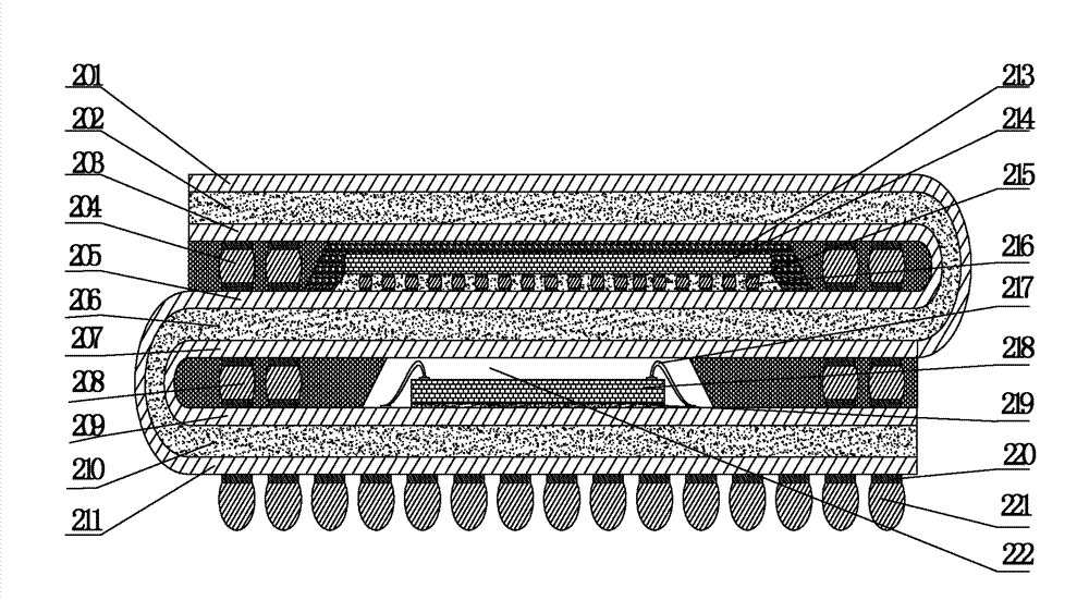
[0059] In the packaging system provided by this embodiment, the substrate inside is also a flexible substrate. The difference from Embodiment 2 is that the flexible substrate described in this embodiment is bent into a Z-shape (or S-shape), and the inside The two components do not interfere with each other, and neither interferes with the external electromagnetic field.

[0060] see image 3 , the packaging system provided in this embodiment includes: a zigzag substrate formed by bending the same flexible substrate, and the zigzag substrate includes: a first substrate 210, a second substrate 206 and a third substrate arranged in sequence The substrate 202 and the second substrate 206 are respectively connected to the first substrate 210 and the third substrate 202 through two bends.

[0061] The first shielding layer 209 is arranged on the side of the first substrate 210 facing the second substrate 206, the second shielding layer 207 is arranged on the side of the second subs...


PUM


Abstract

The invention discloses a sealing system. The sealing system comprises a first baseplate, a second baseplate, a first shielding layer, a second shielding layer, a first component and shielded welding balls. The first baseplate and the second baseplate are oppositely arranged. The first shielding layer is arranged on one surface of the first baseplate and faces the second baseplate. The second shielding layer is arranged on one surface of the second baseplate and faces the first baseplate. The first shielding layer and the second shielding layer are both connected with ground or a power supply. The first component is located on the first shielding layer. The shielded welding balls are located on the periphery of the first shielding layer. The sealing system can effectively solve the problem of electro magnetic compatibility (EMC) and improves sensitivity of the system on the premise of not increasing the size of the system.

Description

technical field [0001] The present invention relates to the technical field of integrated circuit packaging technology, and more specifically, relates to a packaging system. Background technique [0002] With the rise of communication electronics, the demand for miniaturized systems is becoming more and more significant. At present, the packaging technologies used in realizing miniaturized systems mainly include system-in-package (SIP) and package-on-package (POP). The substrate used in the packaging process can be a rigid substrate or a flexible substrate. At present, rigid substrates are widely used, but because flexible substrates are more flexible and thin-film than rigid substrates, and retain the characteristics of insulation and high strength of rigid substrates, their application prospects will be broader. [0003] Flexible substrates are mainly used in three aspects: flexible displays, thin-film solar cells and electronic skins. At the SID conference held in 2007...

Claims


Application Information

Patent Timeline
IPC IPC(8): H01L23/552H05K9/00H01L23/31
CPCH01L2224/73265H01L2224/16225H01L2224/73204H01L2224/48227H01L2224/32225H01L2924/15331H01L2924/3025H01L24/73
Inventor 曹立强郭学平李君陶文君
Owner NAT CENT FOR ADVANCED PACKAGING
Why Eureka
Try Eureka