Diffusion-free avalanche photodiode and preparation method thereof

An avalanche photoelectric and diode technology, applied in circuits, electrical components, semiconductor devices, etc., can solve the problems of limited suppression effect, complex process design, and complicated method realization process, and achieve the effect of reducing surface leakage current and improving reliability.

Active Publication Date: 2015-05-20
WUHAN TELECOMM DEVICES
View PDF2 Cites 0 Cited by
  • Summary
  • Abstract
  • Description
  • Claims
  • Application Information

AI Technical Summary

Problems solved by technology

However, the above-mentioned methods of suppressing edge breakdown all require complex process design, and require precise control of parameters such as diffusion concentration and depth. The implementation process of the method is extremely complicated, and the suppression effect achieved by the method is also very limited.

Method used


Image

  • Diffusion-free avalanche photodiode and preparation method thereof
  • Diffusion-free avalanche photodiode and preparation method thereof
  • Diffusion-free avalanche photodiode and preparation method thereof

Examples


Embodiment Construction

[0047] The present invention will be further described below in conjunction with the accompanying drawings and specific embodiments, so that those skilled in the art can better understand the present invention and implement it, but the examples given are not intended to limit the present invention.

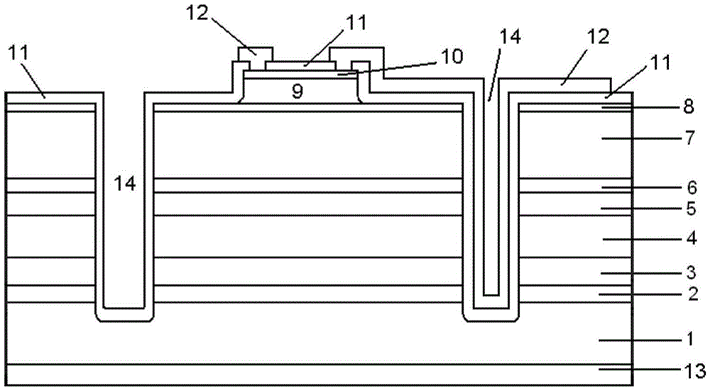
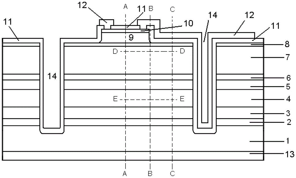
[0048] A kind of diffusion-free avalanche photodiode provided in this embodiment, such as figure 1 and figure 2As shown, a buffer layer 2, a diffusion barrier layer 3, an avalanche multiplication layer 4, an electric field control layer 5, a graded layer 6, a light absorption layer 7, an etch stop layer 8, a window layer 9 and a contact layer 10 are sequentially grown on a substrate 1 . The substrate 1 is preferably a p-InP substrate. The buffer layer 2 is preferably a p-InP buffer layer. The diffusion barrier layer 3 is a p-type doped layer, and the material of the diffusion barrier layer 3 is preferably AlInAs, AlGaInAs or InGaAsP, or a combination of two or more of the abov...


PUM


Abstract

The invention provides a diffusion-free avalanche photodiode and a preparation method thereof. The avalanche photodiode comprises a substrate. A buffer layer, a diffusion impervious layer, an avalanche multiplication layer, an electric field control layer, a gradual change layer, a light absorption layer, a corrosion stop layer, a window layer and a contact layer sequentially grow on the surface of the substrate. The window layer is placed at the central position of the corrosion stop layer. Medium insulating layers of the corrosion stop layer are covered both on the periphery of the window layer and above the contact layer, and the medium insulating layers are provided with annular channels. The circular window layer is corroded by selectivity corrosion, the medium insulating layers are covered on the parts outside the window layer, the size of the window layer can directly define the light sensitive area of the avalanche photodiode, and so that the avalanche photodiode is suitable for working at different rate environments. In addition, although a slightly strong electric field exists on one side, close to the edge of the window layer, of the light absorption layer, edge punch-through can not occur on the avalanche multiplication layer.

Description

technical field [0001] The invention belongs to the technical field of chip manufacturing, and in particular relates to a diffusion-free avalanche photodiode and a preparation method thereof. Background technique [0002] Avalanche photodiodes use a high electric field to accelerate electrons or hole carriers, causing the carriers to collide with the crystal lattice, ionizing secondary electrons or hole carriers, and the secondary carriers drift out of the depletion region to achieve Amplification of the photocurrent. In the field of optical communication applications, avalanche photodiodes, as a high-sensitivity receiving device, are widely used in G-PON / E-PON access optical networks and medium-to-long-distance long-distance trunk transmission. Most of the avalanche photodiodes based on InP substrates adopt the method of sequentially growing n-InP buffer layer, InGaAs light absorption layer, n-InP electric field control layer and low-doped n-InP window layer on n-InP subst...

Claims


Application Information

Patent Timeline
Patent Type & Authority Patents(China)
IPC IPC(8): H01L31/107H01L31/18
Inventor 岳爱文胡艳李晶王任凡
Owner WUHAN TELECOMM DEVICES
Why Eureka
Try Eureka