Scribing method and scribing device

A technology for scribing and scratching depth, applied in welding equipment, laser welding equipment, metal processing equipment, etc., can solve problems such as increased production costs, increased defective rate, edge collapse, etc., to reduce production costs and reduce defective products rate, reduce the effect of chipping

Active Publication Date: 2015-05-20
HANS LASER TECH IND GRP CO LTD
View PDF6 Cites 0 Cited by
  • Summary
  • Abstract
  • Description
  • Claims
  • Application Information

AI Technical Summary

Problems solved by technology

However, due to the particularity of the internal crystal structure of the LED wafer, the fixed scribing depth value makes it easy to cause chipping, micro-cracks, delamination and other damage when the LED wafer is separated by pressure from the cylindrical roller, making the secondary Increased product yield, thereby increasing production costs

Method used


Image

  • Scribing method and scribing device
  • Scribing method and scribing device
  • Scribing method and scribing device

Examples


Embodiment Construction

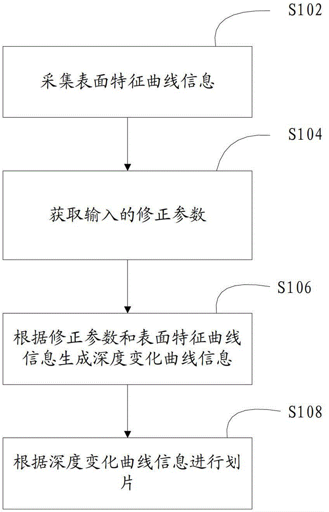
[0037] In one embodiment, such as figure 1 Shown, a kind of dicing method comprises the following steps:

[0038] Step S102, collecting surface characteristic curve information.

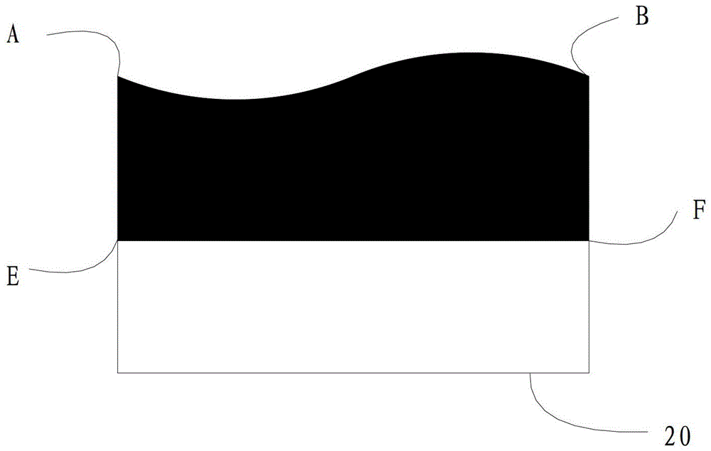
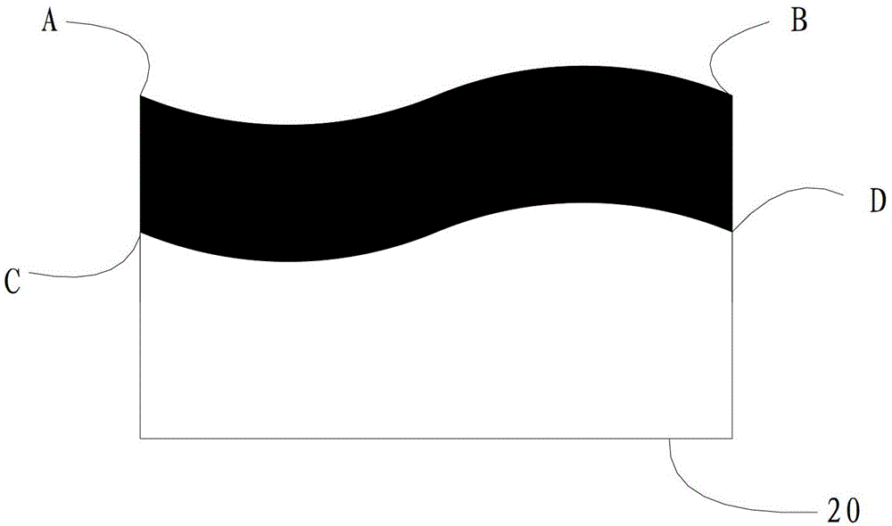
[0039] The surface characteristic curve information is the curve with undulations caused by the different thickness of the surface of the cutting object. For example, if figure 2 As shown, 20 is the wafer as the object to be cut, and curves A to B are the thickness change information of the upper surface at the cross section of the wafer. In this embodiment, the characteristic data of the surface of the cutting object can be collected by a displacement sensor, a scanner or a photoelectric conversion device, and then the surface characteristic curve information can be obtained through signal processing methods such as smoothing and filtering.

[0040] Step S104, acquiring the input correction parameters.

[0041] The correction parameter is the input parameter information. The correction paramet...


PUM


Abstract

A scribing method comprises collecting surface characteristic curve information, obtaining an inputted corrected parameter, generating depth change curve information according to the surface characteristic curve information and the inputted corrected parameter, and scribing according to the depth change curve information. Besides, a scribing device is further provided. The scribing method and the scribing device can reduce defective rate.

Description

technical field [0001] The invention relates to the field of laser precision machining, in particular to a scribing method and device. Background technique [0002] In the traditional LED wafer processing industry, LED wafers need to be diced. The scribing device can draw shallow marks with a certain scribing depth on the surface of the LED wafer. The diced LED wafer can be placed on a flexible support pad, and pressure can be applied to it by a cylindrical roller, so that the LED wafer can be successfully separated. [0003] However, the surface of the LED wafer is not flat, and the edge of its cross section is irregularly curved, so that the scribing device needs to adjust the scribing depth. The scribing method in the traditional technology usually collects the thickness of multiple sampling points on the surface of the LED wafer, calculates the average value of the thicknesses of the multiple sampling points, and then sets a fixed scribing depth according to the averag...

Claims


Application Information

Patent Timeline
Patent Type & Authority Patents(China)
IPC IPC(8): B23K26/36B23K26/70
Inventor 高昆李瑜叶树铃庄昌辉陈红邴虹高云峰
Owner HANS LASER TECH IND GRP CO LTD
Why Eureka
Try Eureka