Capacitive touch screen and manufacturing method thereof

A technology of capacitive touch screen and manufacturing method, which is applied to the input/output process of electrical digital data processing, instruments, and data processing, etc., can solve the problems of inability to use plastic substrates, poor high temperature resistance, and difficulty in reducing the cost of capacitive touch screens. Guaranteed conductivity and light transmittance, reduced manufacturing cost, high flexibility

Active Publication Date: 2013-05-29
SHANTOU GOWORLD DISPLAY TECH CO LTD
View PDF5 Cites 19 Cited by
  • Summary
  • Abstract
  • Description
  • Claims
  • Application Information

AI Technical Summary

Problems solved by technology

[0004] However, this kind of transparent conductive material film generally needs to be deposited at high temperature, so the high temperature resistance of the substrate and other film layers on the capacitive touch screen has been put forward higher requirements, for example, in order to deposit this transparent conductive material on the substrate The thin film of the material needs to use a relatively high temperature resistant glass substrate instead of a plastic substrate, and other film layers on the substrate, such as organic coatings and mimeograph layers, generally have poor high temperature resistance. Afterwards, it is manufactured, which reduces the flexibility of the capacitive touch screen in terms of material, structure, and process selection, making it difficult to reduce the cost of this capacitive touch screen.

Method used


Image

  • Capacitive touch screen and manufacturing method thereof
  • Capacitive touch screen and manufacturing method thereof
  • Capacitive touch screen and manufacturing method thereof

Examples


Embodiment 1

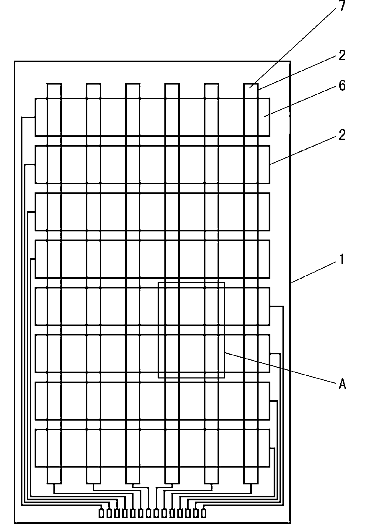
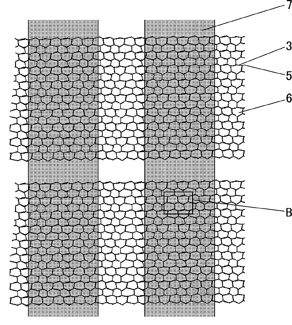
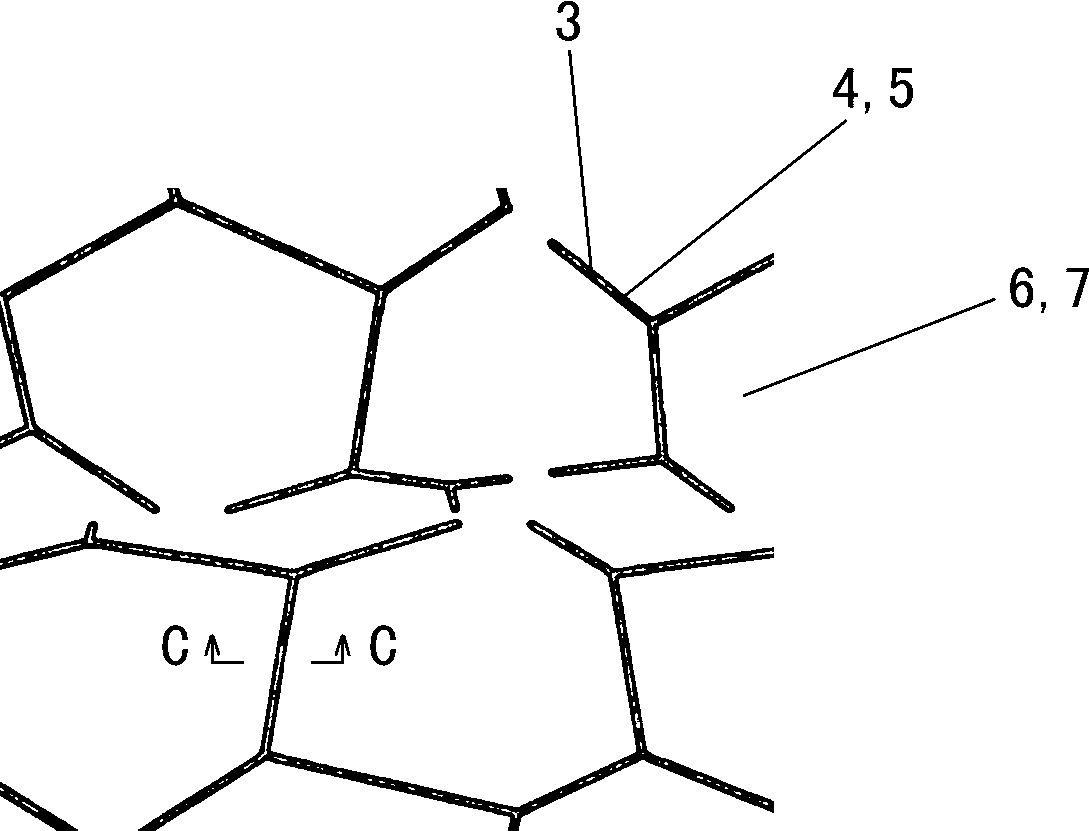
[0051] Such as Figure 1-Figure 4 As shown, this capacitive touch screen includes a glass substrate 1, an electrode layout area 2 is provided on both surfaces of the glass substrate 1, and a plurality of grooves 3 are arranged on the electrode layout area, and the grooves 3 are filled with paste of conductive nanoparticles. body 4 (such as nano-carbon particles, nano-gold and silver particles, etc.), the paste 4 of conductive nanoparticles in each groove 3 is connected to each other to form conductive thin wires 5, which are formed by mesh-like tiling For the sensing electrodes of the capacitive touch screen, a first sensing electrode 6 is formed on one surface of the glass substrate 1 , and a second sensing electrode 7 is formed on the other surface of the glass substrate 1 .

[0052] Taking the first electrode as an example, such as Figure 5 a- Figure 5 As shown in g, its manufacturing method comprises the steps:

[0053] 1), such as Figure 5 As shown in a, a layer of...

Embodiment 2

[0061] Such as Figure 6-Figure 8 As shown, the structure of an integrated capacitive touch screen is adopted, the substrate is a plastic substrate 11, and the sensing electrodes are made on the back of the plastic substrate 11, and the plastic substrate 11 also serves as a protective plate, and the electrode layout area 12 is set on the plastic substrate. On the back side of 11, the sensing electrodes adopt a complementary triangular design, and a plurality of grooves 13 are arranged on the electrode layout area 12, (refer to image 3 , Figure 4 ) The grooves 13 are filled with paste 4 of conductive nanoparticles (such as nano-carbon particles, nano-gold and silver particles, connections of nano-carbon particles, etc.), and the paste 4 of conductive nanoparticles in each groove 13 is connected to each other The conductive thin wires 5 are formed, and the conductive thin wires 5 form the sensing electrodes of the capacitive touch screen by means of grid-like tiling, and the ...

Embodiment 3

[0067] Under the situation that other parts are all identical with embodiment two, its difference is: as Figure 11 , Figure 12 As shown, a plurality of first electrode arrangement regions 31 extending in the same direction are provided on one surface of the plastic substrate 11, and a second electrode arrangement region 32 arranged on one side of each first electrode arrangement region 31, the first electrodes The layout area 31 and the second electrode layout area 32 are all provided with a plurality of grooves 33. After the paste 4 of conductive nanoparticles is filled in the grooves 33, the conductive nanoparticles in the grooves 33 on each first electrode layout area 31 The paste 4 constitutes the first sensing electrode 34 , and the paste 4 of conductive nanoparticles in the grooves 33 on each second electrode arrangement area 32 constitutes the second sensing electrode 35 .


PUM


Abstract

The invention relates to a capacitive touch screen and a manufacturing method thereof. The capacitive touch screen comprises at least one rigid transparent base plate, and is characterized in that at least one surface of each base plate is provided with an electrode arrangement area, each electrode arrangement area is provided with a plurality of grooves, conductive nano-powder is filled in the grooves, the conductive nano-powder in the grooves is connected to form conductive fine wires, and the conductive fine wires form inductive electrodes of the capacitive touch screen in a netted and tiled mode. The inductive electrodes of the capacitive touch screen are manufactured through the method that the grooves are arranged and the conductive nano-powder is embedded into the grooves to form the conductive fine wires, the method that film coating is carried out on the base plate at high temperature does not need to be adopted, and therefore the capacitive touch screen has high flexibility in material, structure and technological selection, and manufacturing cost of the capacitive touch screen is further reduced.

Description

technical field [0001] The present invention relates to a touch screen, in particular to a capacitive touch screen and a corresponding manufacturing method. Background technique [0002] As an efficient input device, the capacitive touch screen has many advantages such as high sensitivity, no force required for touch, and easy multi-touch. It has been applied to various consumer electronic products such as mobile phones, tablet computers, and notebooks. [0003] Structurally speaking, current capacitive touch screens generally include at least one transparent hard substrate and sensing electrodes fabricated on the substrate. These sensing electrodes can be arranged in a matrix or in a triangular design (refer to published patent US4087625), Single-layer design, double-layer or multi-layer design can be adopted. In any case, in order to ensure light transmission, the sensing electrodes need to be made of transparent conductive materials, such as thin films of indium tin oxid...

Claims


Application Information

Patent Timeline
Patent Type & Authority Applications(China)
IPC IPC(8): G06F3/044
Inventor 吴永俊沈奕吕岳敏林钢詹前贤孙楹煌吴锡淳林伟浩
Owner SHANTOU GOWORLD DISPLAY TECH CO LTD
Why Eureka
Try Eureka