Crystalline silicon solar cell with low series resistor and preparation method thereof

A technology of solar cells and series resistance, which is applied in the field of solar cells, can solve the problems of increased battery series resistance, increased electrode resistance, and reduced electrode cross-sectional area, to reduce series resistance, reduce recombination rate, and optimize passivation performance Effect

Inactive Publication Date: 2011-08-31
SUN YAT SEN UNIV
View PDF4 Cites 22 Cited by
  • Summary
  • Abstract
  • Description
  • Claims
  • Application Information

AI Technical Summary

Problems solved by technology

However, a decrease in the width of the fine grid naturally causes a decrease in the cross-sectional area of ​​the electrode, which leads to an increase in the resistance of the electrode, that is, the increase in the series resistance of the battery

Method used


Image

  • Crystalline silicon solar cell with low series resistor and preparation method thereof
  • Crystalline silicon solar cell with low series resistor and preparation method thereof
  • Crystalline silicon solar cell with low series resistor and preparation method thereof

Examples


Embodiment 1

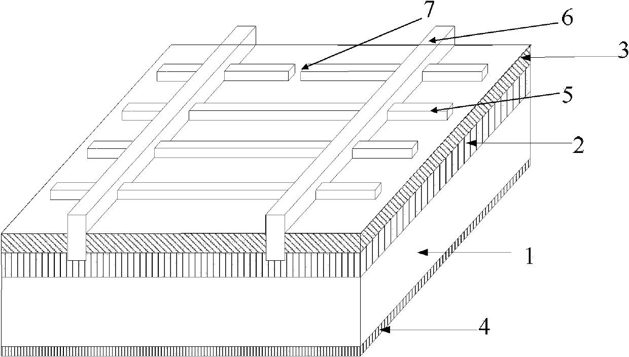
[0032] as attached Figure 1-5 As shown, a crystalline silicon solar cell with low series resistance provided in this embodiment includes a p-n junction p region 1, a p-n junction n region 2, a passivation layer 3 and a thin gate line are arranged on the p-n junction n region 2 The metal electrode 5 and the main grid metal electrode 6 are provided with a back electric field and a back electrode 4 on the p-n junction p region 1, wherein the fine grid line metal electrode 5 and the busbar metal electrode 6 communicate with the p-n junction n region 2 , the back electric field and the back electrode 4 communicate with the p-n junction p region 1, and a transparent conductive film is provided on the front surface of the solar cell, that is, the passivation layer 3, the thin grid metal electrode 5 and the entire area on the main grid metal electrode 6 .

[0033] Among them, the crystalline silicon solar cell in the present invention has the structure of a general crystalline silic...

Embodiment 2

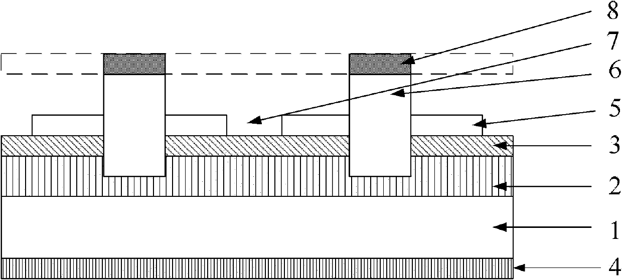
[0035] as attached Figure 1-5 As shown, a crystalline silicon solar cell with low series resistance provided in this embodiment includes a p-n junction p region 1, a p-n junction n region 2, a passivation layer 3 and a thin gate line are arranged on the p-n junction n region 2 The metal electrode 5 and the main grid metal electrode 6 are provided with a back electric field and a back electrode 4 on the p-n junction p region 1, wherein the fine grid line metal electrode 5 and the busbar metal electrode 6 communicate with the p-n junction n region 2 , the back electric field and the back electrode 4 communicate with the p-n junction p region 1, and a transparent conductive film is provided on the front surface of the solar cell, that is, the passivation layer 3, the fine grid metal electrode 5 and the partial area on the main grid metal electrode 6 .

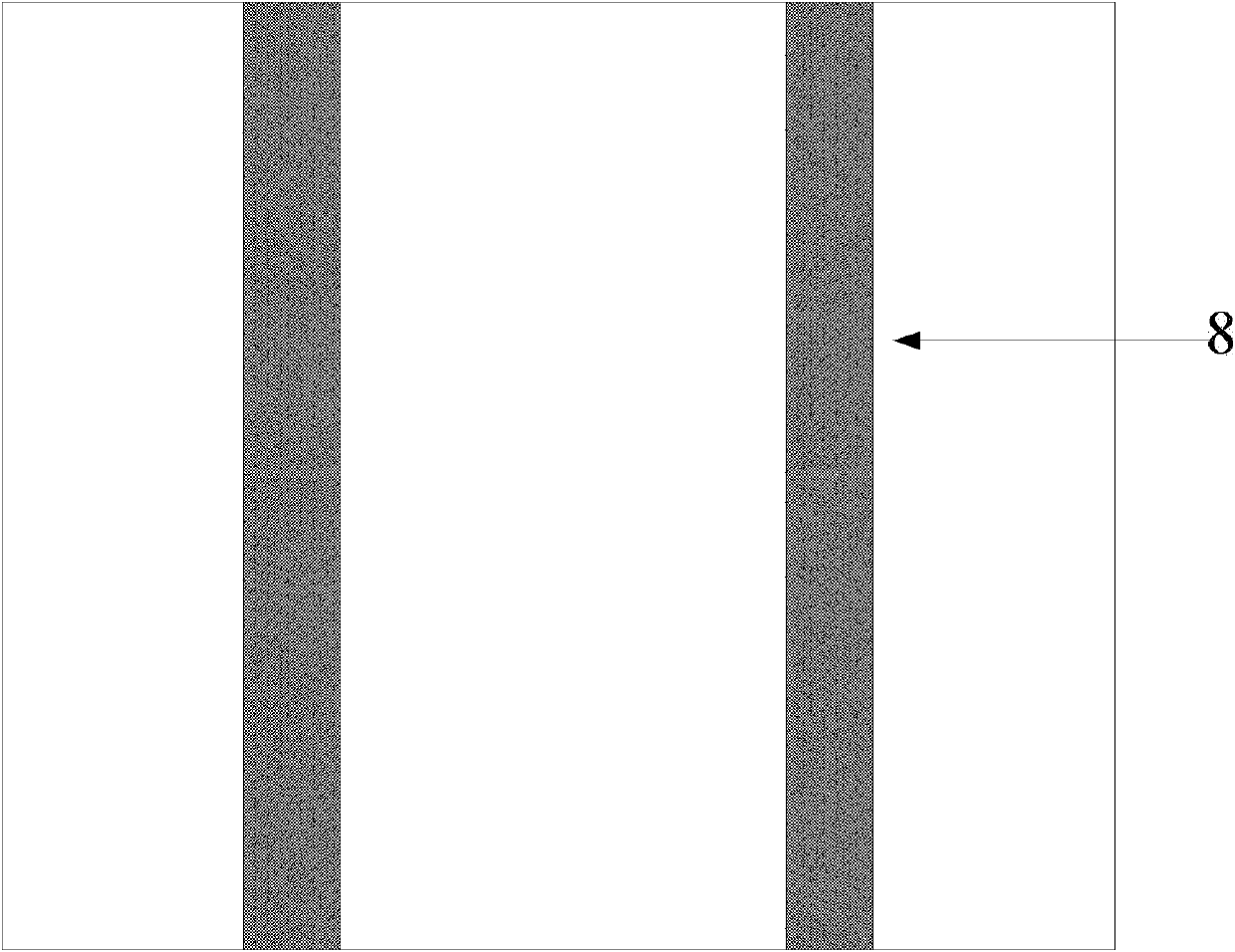
[0036]Among them, by setting a mask on the front surface of the crystalline silicon solar cell and then setting a transparent ...

Embodiment 3

[0038] as attached Figure 1-5 As shown, the general processing steps of a method for preparing a crystalline silicon solar cell with low series resistance are: select the cell, select whether to use a mask and the pattern of the corresponding mask according to actual needs. Use a mask to selectively cover the target area on the front surface of the solar cell, and then use a coating device to plate a transparent conductive film on the area not covered by the mask. Taking mask design as an example, the specific steps are as follows:

[0039] (1) Select the battery. The battery can be a single crystal battery, a polycrystalline battery or a broken grid battery. Take the broken grid battery as an example, such as figure 1 As shown, the battery includes a p-n junction p region 1, a p-n junction n region 2, and a passivation layer 3 is provided on the p-n junction n region 2. The passivation layer 3 can be used by evaporation, sputtering, deposition, ion plating or CVD One or m...


PUM


Abstract

The invention relates to a crystalline silicon solar cell with low series resistor, which comprises a p-n node; a passivation layer, a thin grating metal electrode and a main grating metal electrode are arranged on the front surface of the p-n node, and a back electric field and a back electrode are arranged on the back surface of the p-n node; the thin grating metal electrode, the main grating metal electrode, the back electric field and the back electrode are communicated with the p-n node; and a transparent conducting film is arranged on the full or partial area of the front surface of the crystalline silicon solar cell. The solar cell has a structure having the transparent conducting film, the metal electrodes and the passivation layer, wherein the transparent conducting film can be used for connecting breaking gates so as to reduce the power loss of the breaking gates; the film can reduce the series resistor on the front surface of the cell and enhance the conducting capability of the cell; simultaneously, the crystalline silicon solar cell can play a role in protecting the metal electrode on the front surface of the cell and prevent the metal electrode from oxidizing; and the reflectivity and the color of the crystalline silicon solar cell can be further controlled by adjusting and controlling the transparent conducting film. The invention further discloses a preparation method of the crystalline silicon solar cell.

Description

technical field [0001] The invention belongs to the technical field of solar cells, and in particular relates to a crystalline silicon solar cell with low series resistance and a preparation method thereof. Background technique [0002] At present, the conventional process of preparing crystalline silicon solar cells generally uses screen printing to prepare metal electrodes. During the printing process, the screen may be blocked due to reasons such as too large slurry particles, too long residence time, or aging of the screen, so that metal electrodes, especially The fine grid line metal electrode (finger) is incomplete, forming a broken grid. Meanwhile, the metal electrodes sit on top of crystalline silicon solar cells and are prone to oxidation without any protection. [0003] In order to reduce the shielding of light by the electrodes, the design of high-efficiency cells puts forward higher requirements on the width of the fine-grid electrodes. However, the reduction o...

Claims


Application Information

Patent Timeline
Patent Type & Authority Applications(China)
IPC IPC(8): H01L31/0224H01L31/048H01L31/18B41M1/12
CPCY02E10/50Y02P70/50
Inventor 沈辉陈奕峰洪瑞江
Owner SUN YAT SEN UNIV
Why Eureka
Try Eureka