Display device and driving module thereof, voltage control circuit and method

A voltage control circuit and display device technology, applied to static indicators, instruments, etc., can solve serious problems, such as the drop of output current of thin film transistors, and the failure of liquid crystal display device 100 to display normally.

Active Publication Date: 2013-05-29
AU OPTRONICS CORP
View PDF5 Cites 9 Cited by
  • Summary
  • Abstract
  • Description
  • Claims
  • Application Information

AI Technical Summary

Problems solved by technology

However, when the liquid crystal display device 100 works at a low temperature, the output current of the thin film transistor 124 will drop significantly, thus causing the problem that the liquid crystal display device 100 cannot display normally.
[0005] Among them, in the GOA (Gate Driver on Array) technology that directly integrates the gate driver array on the glass substrate 102, the gate driver array is directly manufactured on the glass substrate 102 through a semiconductor process, instead of an external Integrated drive circuits, but due to semiconductor material limitations, the problem of gate driver arrays 114 and 116 at low temperature start-up is more serious

Method used


Image

  • Display device and driving module thereof, voltage control circuit and method
  • Display device and driving module thereof, voltage control circuit and method
  • Display device and driving module thereof, voltage control circuit and method

Examples


Embodiment Construction

[0071] The present invention will be described in detail below in conjunction with the accompanying drawings and specific embodiments, but not as a limitation of the present invention.

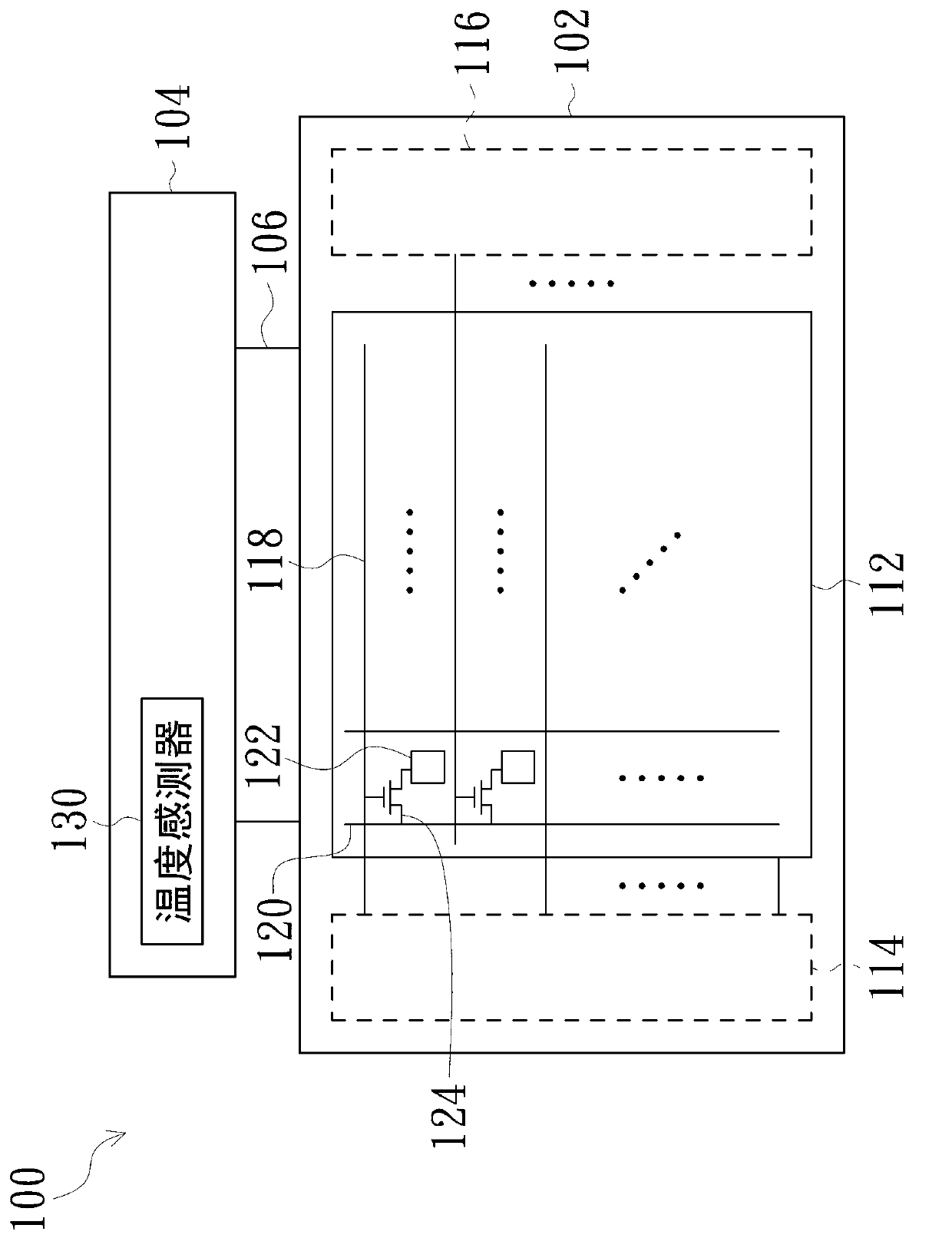
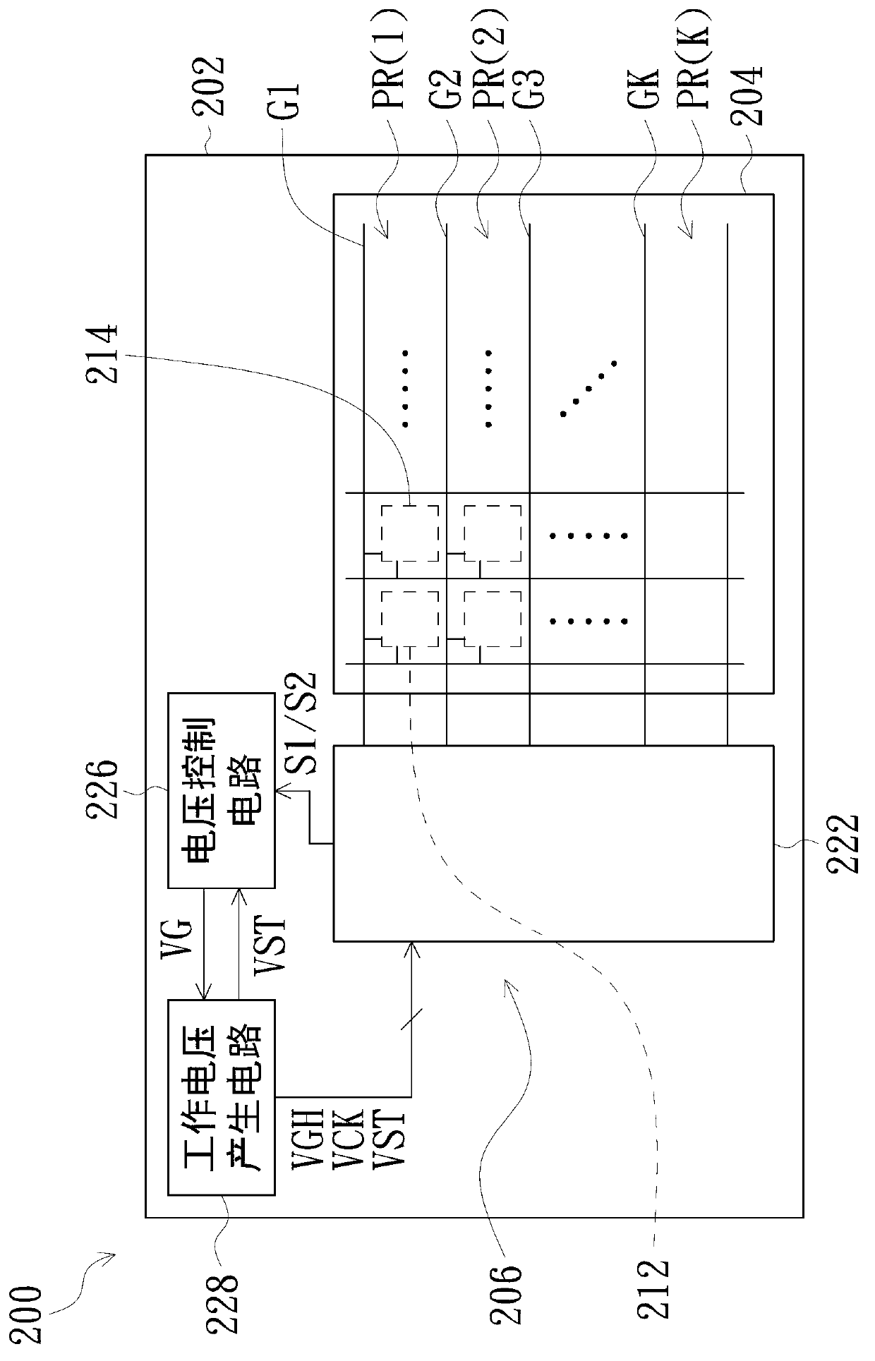
[0072] Figure 2A A block diagram of a display device according to an embodiment of the present invention is shown. Please refer to Figure 2A , the display device 200 provided in this embodiment includes a substrate 202 . In this embodiment, the substrate 202 may be (but not limited to) a glass substrate. In addition, a display area 204 and a driving module 206 are disposed on the substrate 202 . In some embodiments, some components in the driving module 206 do not have to be configured on the substrate 202 .

[0073] The display area 204 has a plurality of pixel columns arranged in sequence, such as PR(1), PR(2) . . . to PR(K), wherein K is a positive integer. In addition, each pixel row corresponds to at least one gate line, such as G1 , G2 , G3 . . . to GK. In each pixel row, a plura...


PUM


Abstract

The present invention relates to a display device and a driving module thereof, a voltage control circuit and method. The voltage control circuit can control an operation voltage of a grid driver array of the display device, and comprises a grid driving pulse generating unit and a controller. The grid driving pulse generating unit generates a grid driving pulse, receives a scanning signal and a reference voltage outputted by the grid driver array, and controls the length of the grid driving pulse according to the level relation of the scanning signal and the reference voltage. The controller is coupled with the grid driving pulse generating unit to receive a grid driving pulse, and controls the level of the operation voltage according to the length of the grid driving pulse.

Description

technical field [0001] The present invention relates to a control method of a display device, and in particular to a control method of a display device for compensating the operating voltage of a gate driver array. Background technique [0002] figure 1 It is shown as an internal block diagram of a conventional liquid crystal display device. Please refer to figure 1 , the existing liquid crystal display device 100 includes a glass substrate 102 and a printed circuit board 104 , and the printed circuit board 104 can be coupled to the glass substrate 102 through a flexible substrate 106 . [0003] On the glass substrate 102 , a display area 112 and gate driver arrays 114 and 116 are included. In the display area 112 , there are a plurality of gate lines 118 and a plurality of source lines 120 , which are alternately arranged in sequence. Wherein, at the intersection of each gate line 118 and each source line 120, a liquid crystal unit 122 is arranged respectively as pixel ...

Claims


Application Information

Patent Timeline
IPC IPC(8): G09G3/36
CPCG09G3/20G09G3/3677G09G3/3696G09G2320/041G09G2320/0666
Inventor 詹秉燏徐智哲陈勇志蔡明谚
Owner AU OPTRONICS CORP
Why Eureka
Try Eureka