Supercharge Your Innovation With Domain-Expert AI Agents!

tft-lcd array substrate and its manufacturing method and display screen

A technology of an array substrate and a manufacturing method, applied in the field of a TFT-LCD array substrate and its manufacturing method, and a display screen, capable of solving the problems of low public voltage acquisition efficiency and achieving the effect of improving acquisition efficiency

Active Publication Date: 2016-09-07
SHANGHAI AVIC OPTOELECTRONICS
View PDF5 Cites 1 Cited by
  • Summary
  • Abstract
  • Description
  • Claims
  • Application Information

AI Technical Summary

Problems solved by technology

[0011] The purpose of the present invention is to provide a TFT-LCD array substrate and its manufacturing method and display screen, so as to solve the problem of low public voltage acquisition efficiency in the prior art

Method used


Image

  • tft-lcd array substrate and its manufacturing method and display screen
  • tft-lcd array substrate and its manufacturing method and display screen
  • tft-lcd array substrate and its manufacturing method and display screen

Examples


Embodiment Construction

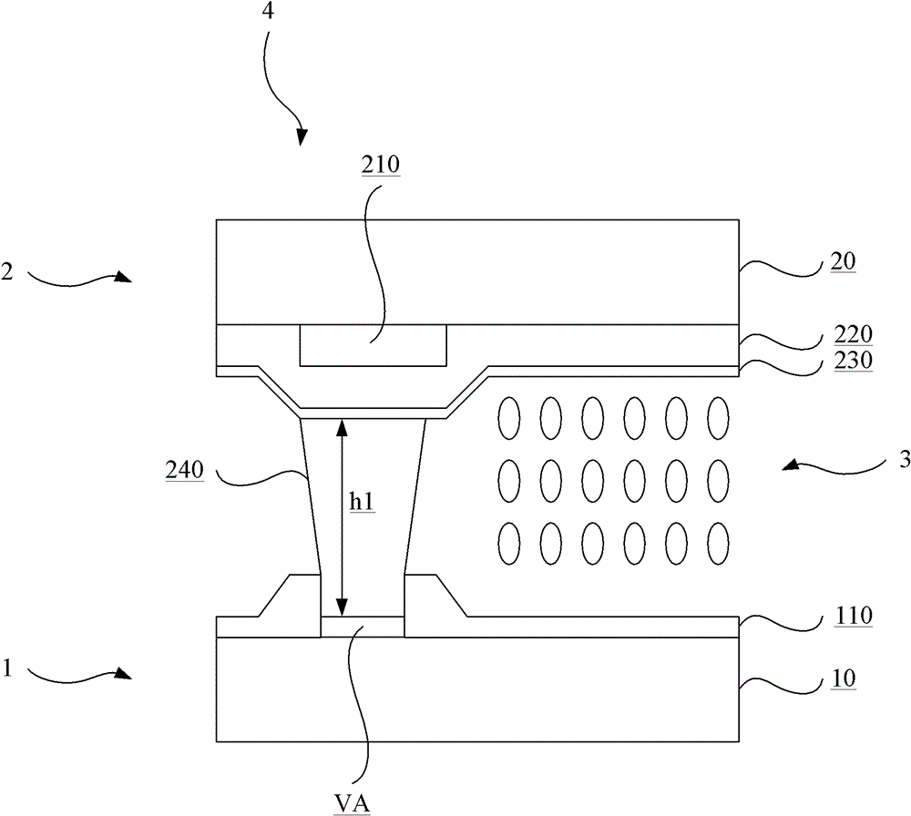
[0048] The TFT-LCD array substrate, its manufacturing method and display screen provided by the present invention will be further described in detail below with reference to the drawings and specific embodiments. Advantages and features of the present invention will be apparent from the following description and claims. It should be noted that all the drawings are in a very simplified form, and are only used for the purpose of conveniently and clearly assisting in describing the embodiments of the present invention.
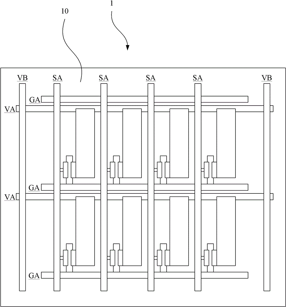
[0049] The core idea of ​​the present invention is to provide a TFT-LCD array substrate and its manufacturing method, and in the display screen, the common electrode bus line is arranged in parallel with the gate line, so that the common electrode bus line and the access line are arranged crosswise, thus, The entire common electrode bus can be used to connect with the access line, so as to obtain the common voltage at multiple points, and improve the efficiency o...


PUM


Abstract

The invention provides a thin film transistor (TFT) - liquid crystal display (LCD) array substrate and a manufacturing method thereof, and a display screen. The array substrate comprises a substrate body, a first metal layer, a gate line, a common electrode bus, a second metal layer, a data line and a common electrode wire, wherein the first metal layer is formed on the substrate body, and the grate line and the common electrode bus are located on the first metal layer and installed in parallel; and the second metal layer is formed on the first metal layer, the data line and the common electrode wire are located on the second metal layer, the data line and the common electrode wire cross the grate line and the common electrode bus, the data line and the common electrode wire are installed in parallel, and the common electrode wire is in electric connection with the common electrode bus. By means of the fact that the common electrode bus and the grate line are installed in parallel, the common electrode bus and an access line are installed in a crossed mode, so that the whole common electrode bus can be used for being connected with the access line. Therefore, common voltage is obtained from multiple points, and obtaining efficiency of the common voltage is improved.

Description

technical field [0001] The invention relates to the technical field of liquid crystal displays, in particular to a TFT-LCD array substrate, a manufacturing method thereof, and a display screen. Background technique [0002] TFT-LCD (Thin Film Transistor Liquid Crystal Display) has the advantages of low voltage, low power consumption, large amount of displayed information, easy colorization, etc., and occupies a dominant position in the current display market. It has been widely used in electronic equipment such as electronic computers, electronic notebooks, mobile phones, video cameras, and high-definition televisions. [0003] One of the most basic components of a TFT-LCD is a display screen, which includes a boxed array substrate and a color filter substrate, and a liquid crystal layer filling the gap between the array substrate and the color filter substrate. The basic principle of displaying images on the display screen is: by applying an electric field acting on the li...

Claims


Application Information

Patent Timeline
IPC IPC(8): G02F1/1362G02F1/1368G02F1/1345G02F1/1335H01L21/77
Inventor 曹兆铿
Owner SHANGHAI AVIC OPTOELECTRONICS
Features
  • R&D
  • Intellectual Property
  • Life Sciences
  • Materials
  • Tech Scout
  • Unparalleled Data Quality
  • Higher Quality Content
  • 60% Fewer Hallucinations
Learn More