Semiconductor device and method of forming the same

A semiconductor and device technology, applied in the field of semiconductor devices and their formation, can solve the problems of large RC effect and poor performance of semiconductor integrated circuits, etc., and achieve the effects of improving performance, reducing RC effect, and solving deposition difficulties

Active Publication Date: 2015-08-05
SEMICON MFG INT (SHANGHAI) CORP
View PDF6 Cites 0 Cited by
  • Summary
  • Abstract
  • Description
  • Claims
  • Application Information

AI Technical Summary

Problems solved by technology

[0010] However, the RC effect of semiconductor devices using the prior art is still large, and the performance of semiconductor integrated circuits is poor

Method used


Image

  • Semiconductor device and method of forming the same
  • Semiconductor device and method of forming the same
  • Semiconductor device and method of forming the same

Examples


no. 1 example

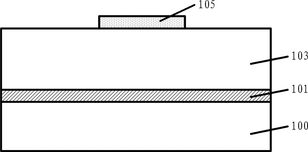
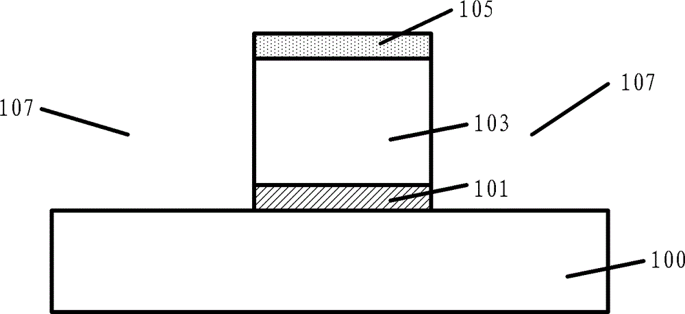
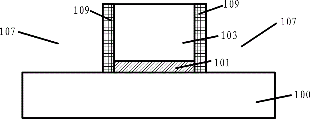
[0067] Please refer to Figure 8 , providing a substrate 300; an etch barrier layer 301 is formed on the surface of the base 300; a first insulating layer 303 is formed on the surface of the etch barrier layer 301; an interlayer dielectric layer 305 is formed on the surface of the first insulating layer 303; A buffer layer 307 is formed on the surface of the interlayer dielectric layer 305 ; a second mask layer 308 is formed on the surface of the buffer layer 307 .

[0068] Wherein, the substrate 300 is used to provide a working platform for subsequent processes, and the part of the substrate 300 in contact with the etching barrier layer is an insulating material. There may also be transistors and the like in the substrate 300 .

[0069] The etch stop layer 301 is used to subsequently protect the substrate 300 from being damaged when the trench 309 is formed, the material of the etch stop layer 301 is SiN or TiN, and the formation process of the etch stop layer 301 is a depos...

no. 2 example

[0116] Different from the first embodiment of the present invention, in the second embodiment of the present invention, at least three grooves need to be formed: a first groove, a second groove adjacent to the first groove, and a groove adjacent to the first groove. The third trench adjacent to the second trench and spaced apart from the first trench forms the first metal line layer, the second trench and the second trench respectively located in the first trench, the second trench and the third trench. The metal line layer and the third metal line layer; the first insulating layer and part of the interlayer dielectric layer between the first metal line layer and the second metal line layer are removed to form an opening, while the second metal line layer remains and the first insulating layer and the interlayer dielectric layer between the third metal line layer.

[0117] Please refer to Figure 15 , providing a substrate 400, an etch barrier layer 401 is formed on the surfa...


PUM

PropertyMeasurementUnit
widthaaaaaaaaaa

Abstract

The invention provides a forming method of a semiconductor device. The forming method comprises steps of providing a substrate, forming a first insulating layer, an interlayer dielectric layer and at least two grooves which penetrate through the interlayer dielectric layer and the first insulating layer in thickness on the surface of the substrate in sequence, filling the grooves with conductive materials to form a metal wire layer, forming a first mask layer which covers the metal wire layer by the adoption of the self alignment forming technology of metal, wherein the first mask layer covers a part, close to the metal wire layer, of the interlayer dielectric layer, using the first mask layer as a mask to remove the interlayer dielectric layer and the first insulating layer to form an opening, and removing the first mask layer to form a second insulating layer which covers the metal wire layer and the interlayer dielectric layer and stretches across the opening. The semiconductor device formed by means of the forming method is provided with a large air gap, reduces a K value in an interconnection structure, reduces an RC effect, and improves the performance of a semiconductor integrated circuit.

Description

technical field [0001] The invention relates to the technical field of semiconductor manufacturing, in particular to a semiconductor device and a forming method thereof. Background technique [0002] As the semiconductor industry enters a new era of high-performance and multi-functional integrated circuits, the density of components in integrated circuits will increase, while the size of components and the spacing between parts or components will decrease accordingly. In the past, it was only limited by the ability of lithographic technology to define the structure, and it was difficult to reduce the geometric size of the device. With the development of technology, the size of existing devices can be made smaller, but there are more and more limiting factors. For example, when the distance between the conductive patterns decreases, the capacitance generated by any two adjacent conductive patterns will increase. This increased capacitance results in increased capacitive coup...

Claims


Application Information

Patent Timeline
Patent Type & Authority Patents(China)
IPC IPC(8): H01L21/768H01L23/525
Inventor 洪中山
Owner SEMICON MFG INT (SHANGHAI) CORP
Why Eureka
Try Eureka