Indium columns for face-down bonding interconnection of infrared focal plane and preparation method thereof

A technology of infrared focal plane and indium pillars, which is applied in the field of reverse soldering interconnection technology of infrared focal plane detectors, can solve problems such as the difficulty of evaporating indium to fill indium pillar holes, short circuit of pixels, and small bottom of indium pillars, etc., so as to avoid sticking The effect of binder residue, good height consistency, and large bottom size

Active Publication Date: 2011-07-27
SHANGHAI INST OF TECHNICAL PHYSICS - CHINESE ACAD OF SCI
View PDF5 Cites 19 Cited by
  • Summary
  • Abstract
  • Description
  • Claims
  • Application Information

AI Technical Summary

Problems solved by technology

The reduction of the pixel center distance requires that the size of the indium column must be reduced. If the size of the indium column is not reduced, the pixels are easily short-circuited due to the deformation of the indium column under pressure during flip soldering interconnection.
Due to the need for reverse soldering interconnection, the height of the indium column cannot be reduced, and it needs to be around 10 microns. If the size of the indium column is reduced, the aspect ratio of the indium column photolithography hole increases during the preparation of the indium column, and the shadow effect will cause evaporation. It is difficult for indium to fill the holes of indium pillars, and it is impossible to obtain indium pillars whose shape and size meet the requirements
Using the existing traditional preparation method, the obtained indium column has a small bottom and a large top, and there is a residual indium layer on the top edge. For an array with a small center-to-center distance, it is easy to short circuit due to the deformation of the indium column during flip soldering interconnection.
Moreover, using traditional photolithography and growth methods, the bottom of the photolithographic indium column hole is small and the top is large, and the indium layer almost fills the indium column hole obtained by photolithography. The high-temperature indium source during growth contacts with the photoresist to generate oxidation. Indium or carbonization of the photoresist, these excesses will remain on the periphery of the indium column, affecting the connectivity consistency of the flip soldering interconnection

Method used


Image

  • Indium columns for face-down bonding interconnection of infrared focal plane and preparation method thereof
  • Indium columns for face-down bonding interconnection of infrared focal plane and preparation method thereof
  • Indium columns for face-down bonding interconnection of infrared focal plane and preparation method thereof

Examples


Embodiment Construction

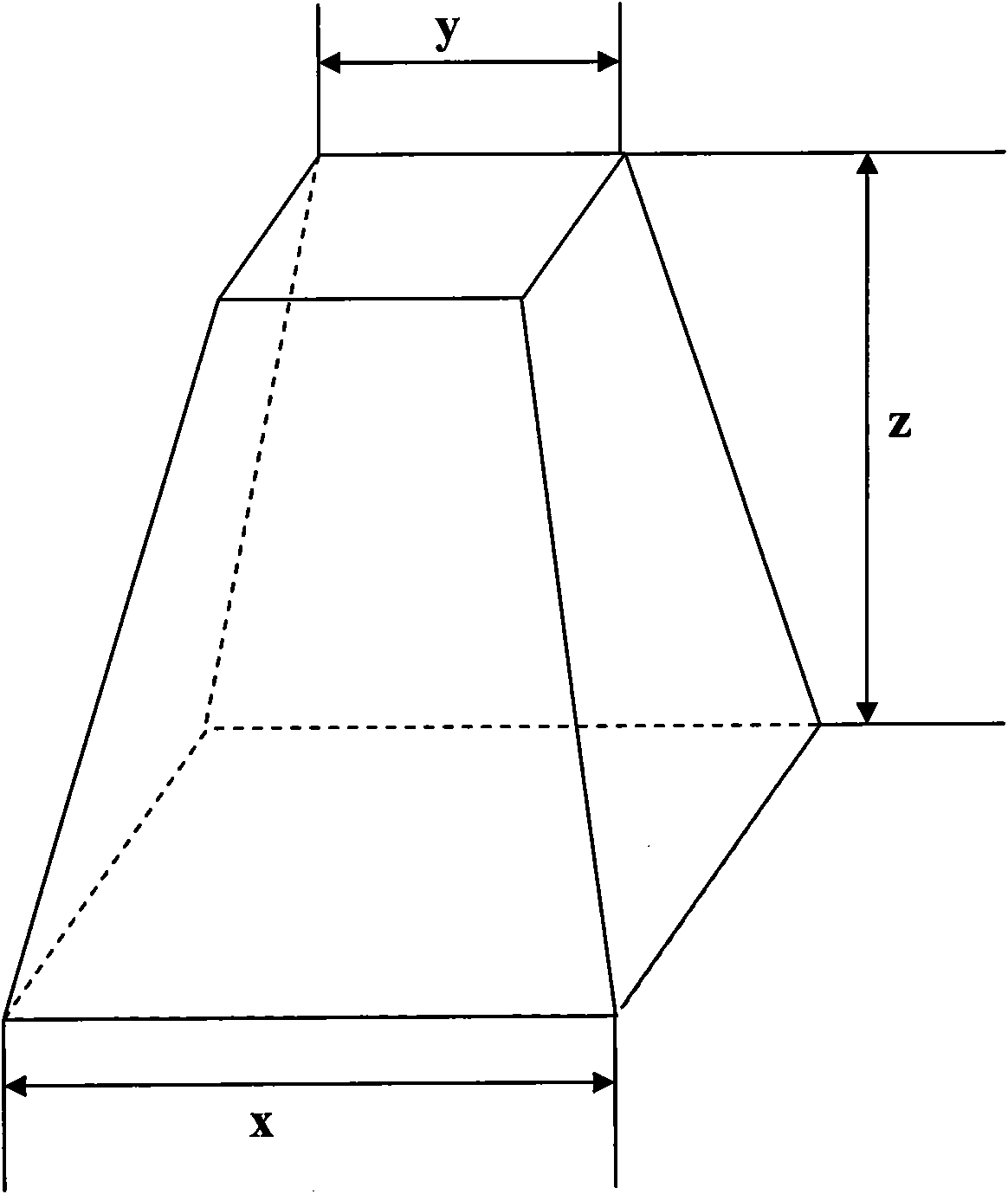
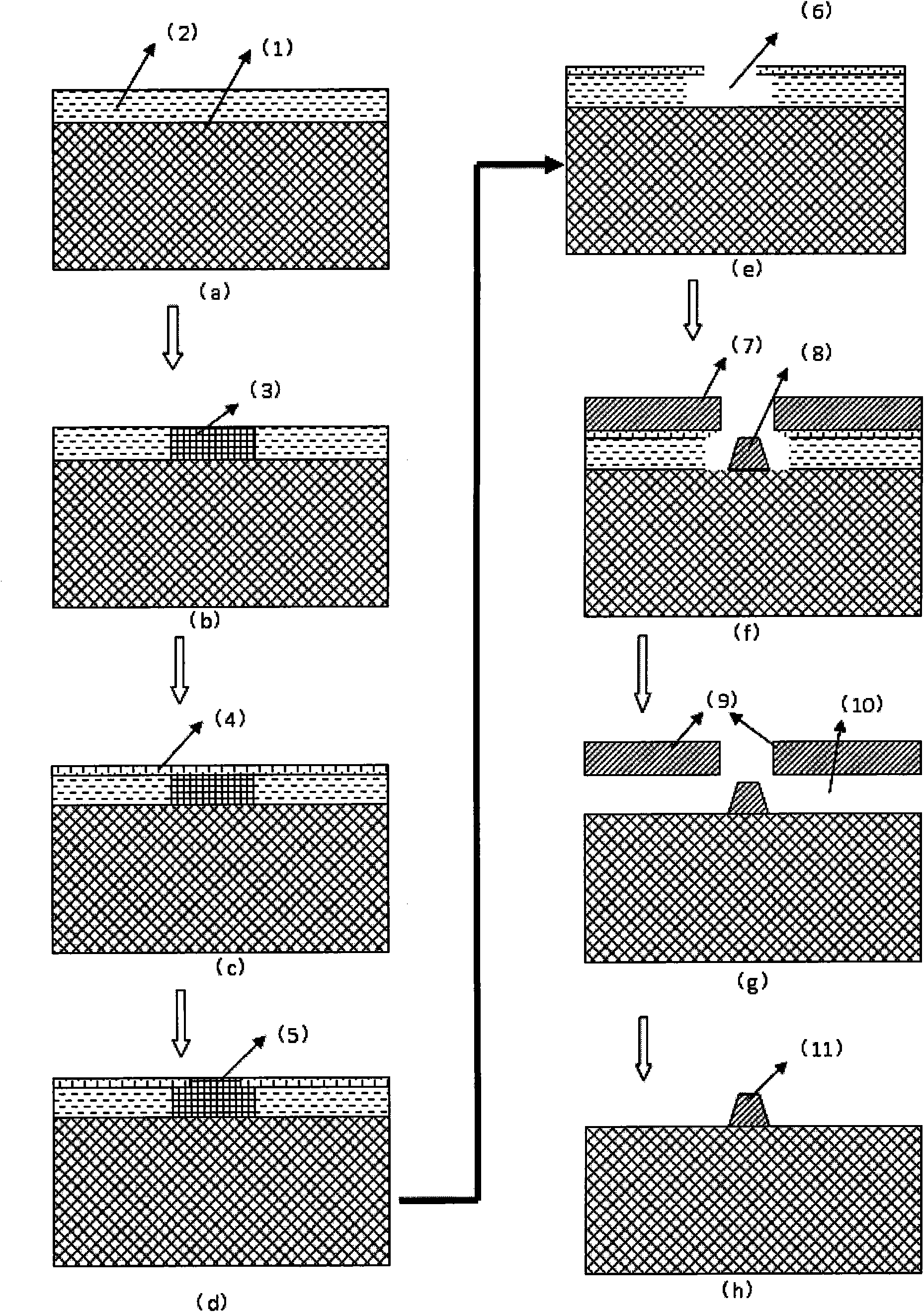
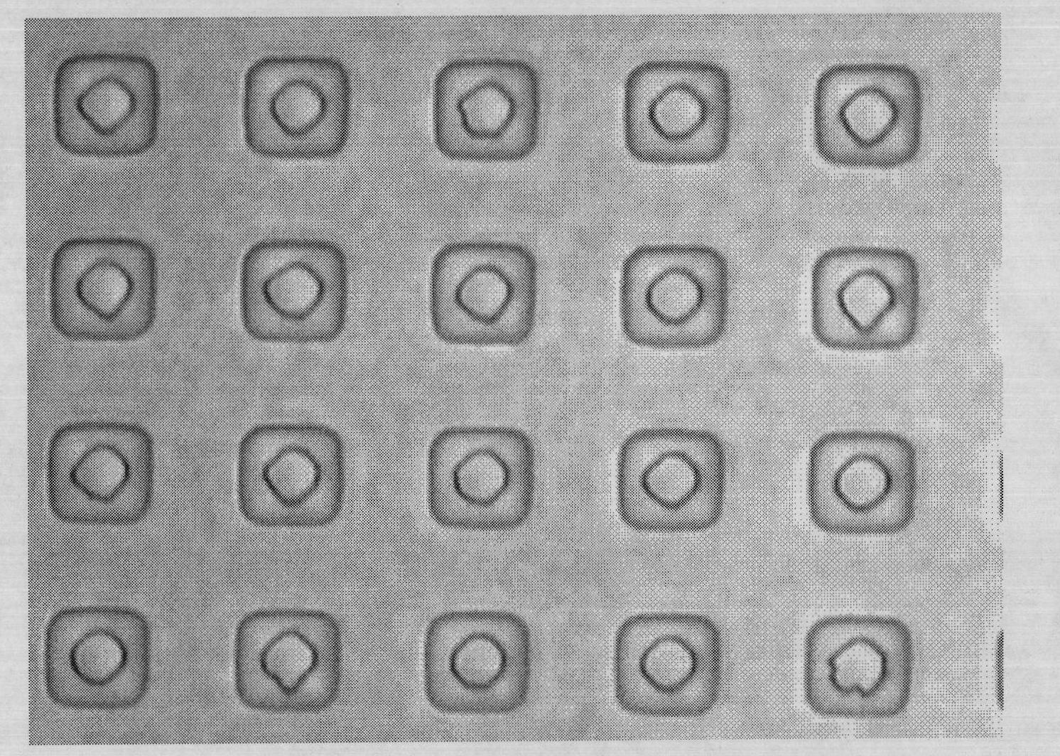
[0027] Below in conjunction with the accompanying drawings, the embodiment of the present invention will be described in detail by taking a chip with a center-to-center distance of 20 microns and an indium column array of 320x240 as an example:

[0028] In an embodiment of the present invention, a mercury cadmium telluride infrared chip on which a gold layer has been grown is used to grow an array of indium pillars. The preparation method of the indium column described in the present invention refers to performing two times of spin-coating photoresist on the mercury cadmium telluride infrared chip that needs to prepare the indium column, two separate exposures, and one development method to carry out the photoresisting of the indium column hole. When the indium layer is deposited by high-vacuum thermal evaporation, it is ensured that the chip is directly above the indium evaporation source. After the indium layer is grown, an organic reagent wet stripping method is used to obta...


PUM

PropertyMeasurementUnit
heightaaaaaaaaaa
heightaaaaaaaaaa
sizeaaaaaaaaaa

Abstract

The invention discloses indium columns for the face-down bonding interconnection of an infrared focal plane and a preparation method thereof. In the method, the spin coating of photoresist and independent exposure are performed twice respectively on a chip of which the indium columns are needed to be prepared, the photoetching of indium column holes are performed by a one-time development method,the chip is positioned right above an indium evaporation source during high-vacuum thermal evaporation deposition of indium layers, and a novel indium column array is obtained in the mode of stripping the grown indium layers by using an organic reagent in a wet process. By the preparation method, the novel indium column array with large bottom size, small top size and high height consistency can be obtained, and the preparation requirement of the indium column array of a small-center distance focal plane detector can be met. The prepared indium columns cannot be contacted with the photoresistin the growth process, the generation of indium oxide or the carbonization of the photoresist due to the contact between a high-temperature indium source and the photoresist in the growth process canbe prevented, and redundant indium layers can be removed by a method of wet stripping by using the organic reagent, so that redundant residues are prevented from being attached to the surfaces of theindium columns.

Description

technical field [0001] The invention relates to an infrared focal plane detector flip-welding interconnection process technology, in particular to an indium column used for infrared focal plane flip-welding interconnection and a preparation method thereof. Background technique [0002] Infrared focal plane detector is an imaging sensor that realizes infrared information acquisition and information processing at the same time, and it has a wide range of applications in military and civilian fields. Due to the important application of infrared focal plane detectors in the military, high-performance and large-scale infrared focal plane arrays have been officially used in various major national security projects in various countries. [0003] As the scale of the infrared focal plane detector array increases, the resolution requirements are getting higher and higher, and the center distance of the pixels is required to be continuously reduced to meet the requirements. The latest ...

Claims


Application Information

Patent Timeline
Patent Type & Authority Applications(China)
IPC IPC(8): H01L27/146H01L31/02H01L31/18G03F7/00B81C1/00
CPCY02P70/50
Inventor 廖清君马伟平朱建妹林春王建新胡晓宁
Owner SHANGHAI INST OF TECHNICAL PHYSICS - CHINESE ACAD OF SCI
Why Eureka
Try Eureka