Power semiconductor device
A technology of power semiconductors and semiconductors, which is applied in the direction of semiconductor devices, semiconductor/solid-state device components, electric solid-state devices, etc. It can solve problems such as difficult long-term use, easy damage to the connection part, and shortened life of power semiconductor devices, achieving light weight , the effect of high heat dissipation efficiency
- Summary
- Abstract
- Description
- Claims
- Application Information
AI Technical Summary
Problems solved by technology
Method used
Image
Examples
no. 1 approach
[0032] (structure)
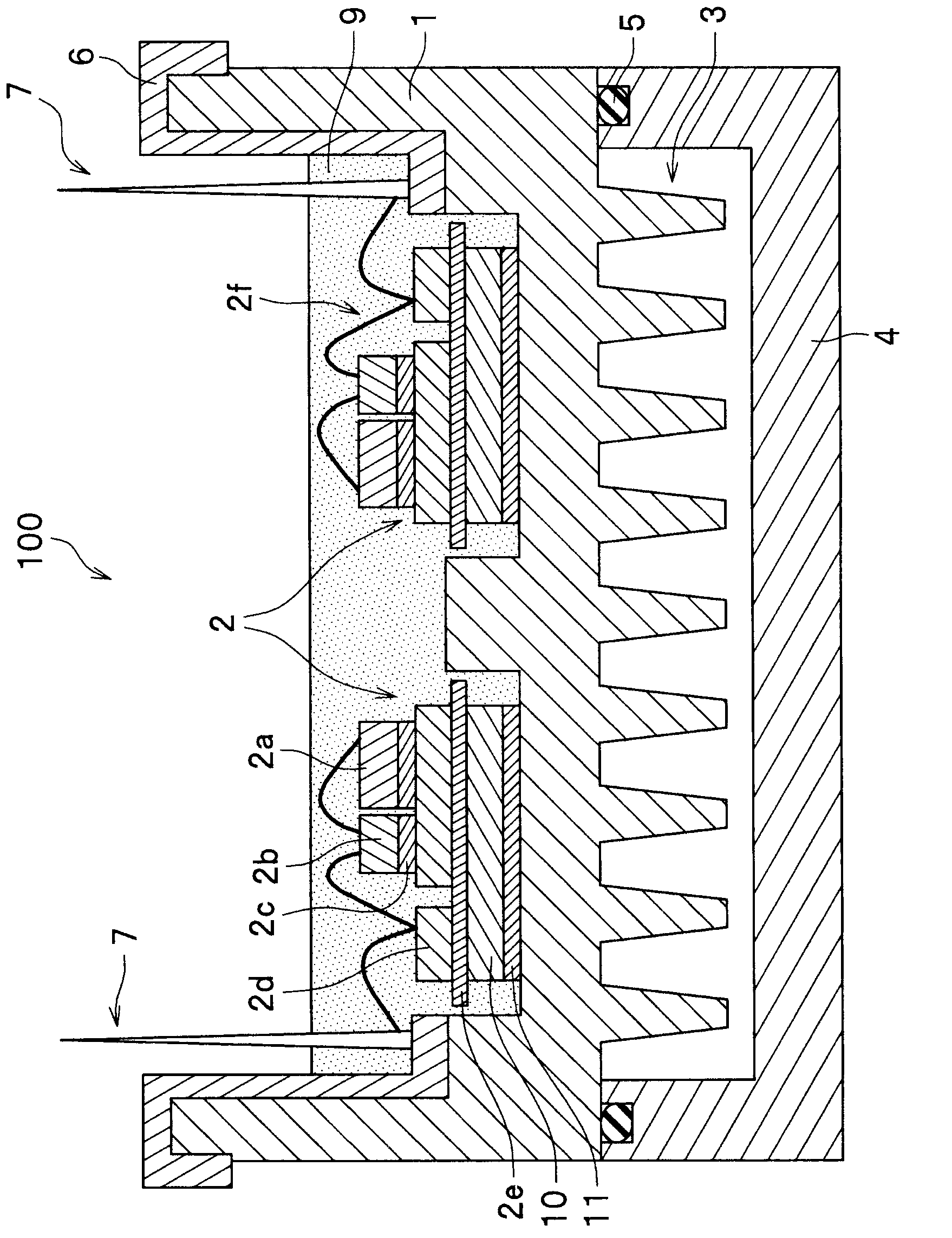
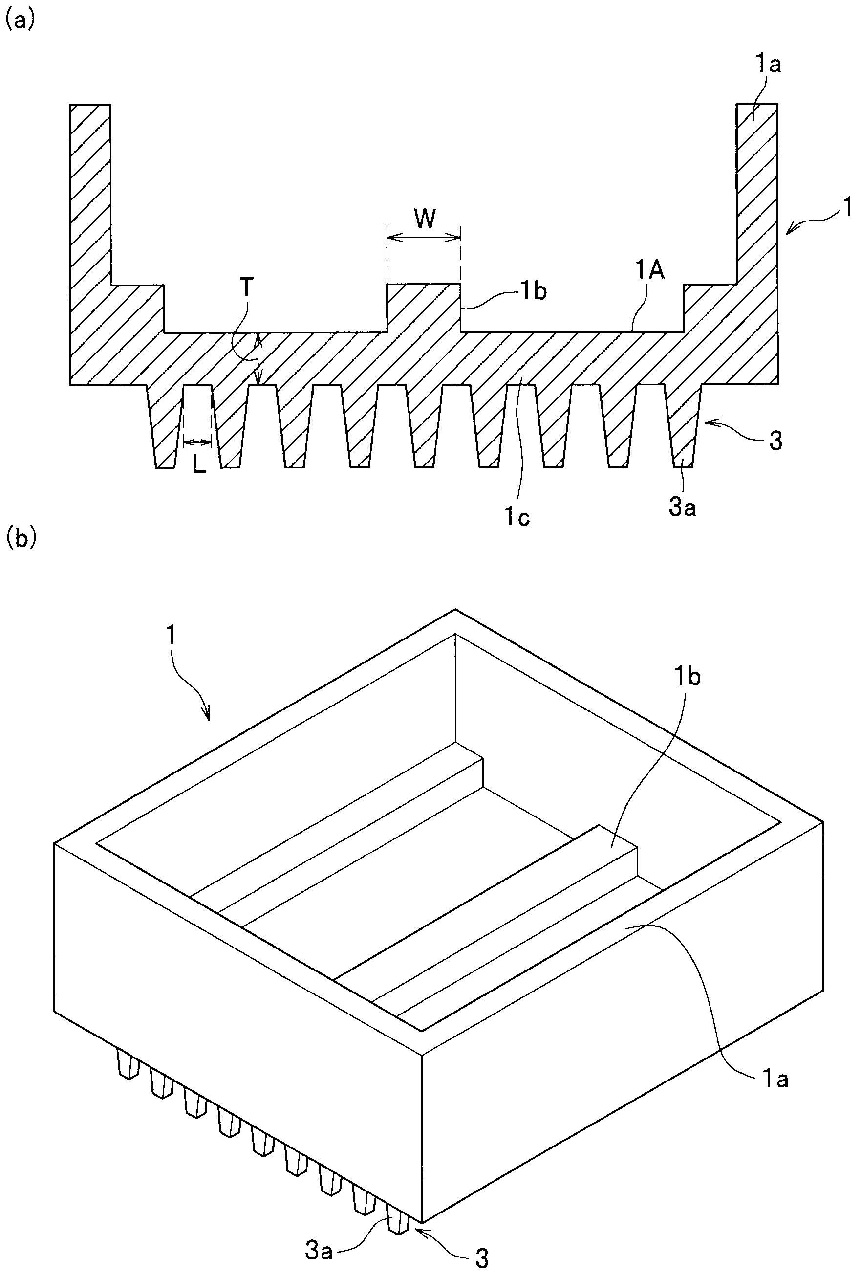
[0033] Such as figure 1 As shown, the power semiconductor device 100 of the first embodiment includes a base body 1 , a semiconductor circuit 2 arranged on the base body 1 , and cooling fins 3 for cooling the semiconductor circuit 2 . Furthermore, the base 1 includes an edge 1a surrounding its periphery, a convex portion 1b formed over the edge 1a in a space surrounded by the edge 1a, and a bottom 1c formed with the convex portion 1b. In addition, the edge part 1a is one form of the "convex part" prescribed|regulated in the scope of protection. Therefore, in the present embodiment, two or more "protrusions" defined in the scope of protection are provided.
[0034] Detailed reference for the edge 1a, convex portion 1b, and bottom 1c figure 2 (a) to be described later.
[0035] Additionally, if figure 1 As shown, the power semiconductor device 100 includes a cooling jacket 14, a sealing member 5, a preform 6, an electrode 7, and wiring 2f. In addition...
no. 2 approach
[0099] Next, refer to Figure 10 The power semiconductor device 200 of the second embodiment will be described. Also, for figure 1 In the illustrated power semiconductor device 100 , the same components are denoted by the same reference numerals, and detailed description thereof will be omitted.
[0100] In the power semiconductor device 200, the height of the convex portion 1b of the power semiconductor device 100 is approximately the same as the height of the edge portion 1a. That is, in the power semiconductor device 100, only one space is surrounded by the edge portion 1a. However, in the power semiconductor device 200, one space surrounded by the edge 1a is divided by the protrusion 1b, and two spaces are formed.
[0101] By forming the convex portion 1b in this way, the height of both the edge portion 1a and the convex portion 1b can be made higher than the height of the silicone gel 9 . Furthermore, even if the power semiconductor device 200 is configured in this wa...
no. 3 approach
[0104] Next, refer to Figure 11 The power semiconductor device 300 of the third embodiment will be described. Also, for figure 1 In the illustrated power semiconductor device 100 , the same components are denoted by the same reference numerals, and detailed description thereof will be omitted.
[0105] In the power semiconductor device 300 , the shape of the cooling fin 3 is different from the shape of the cooling fin 3 of the power semiconductor device 100 . That is, the cooling fin 3 of the power semiconductor device 300 is constituted by a rectangular (plate-shaped) fin 3 b having a gap 3 c. By configuring the cooling fin 3 in this way, the refrigerant can also flow through the gap 3c. Therefore, the contact area of the refrigerant with the rectangular fin 3b becomes larger, and the heat radiation efficiency by the cooling fin 3 can be further improved.
PUM
| Property | Measurement | Unit |
|---|---|---|
| Thickness | aaaaa | aaaaa |
| Length | aaaaa | aaaaa |
| Thermal conductivity | aaaaa | aaaaa |
Abstract
Description
Claims
Application Information
 - R&D Engineer
- R&D Manager
- IP Professional
- Industry Leading Data Capabilities
- Powerful AI technology
- Patent DNA Extraction
Browse by: Latest US Patents, China's latest patents, Technical Efficacy Thesaurus, Application Domain, Technology Topic, Popular Technical Reports.
© 2024 PatSnap. All rights reserved.Legal|Privacy policy|Modern Slavery Act Transparency Statement|Sitemap|About US| Contact US: help@patsnap.com


