Crystal plate stacked structure and manufacturing method thereof

A manufacturing method and wafer technology, which can be used in semiconductor/solid-state device manufacturing, semiconductor/solid-state device components, semiconductor devices, etc., and can solve problems such as warping of stacked wafers

Inactive Publication Date: 2013-06-05
ADVANCED SEMICON ENG INC
View PDF4 Cites 5 Cited by
  • Summary
  • Abstract
  • Description
  • Claims
  • Application Information

AI Technical Summary

Problems solved by technology

[0006] In view of this, the present invention provides a chip stacking structure and its manufacturing method to solve the problem of warping of the corners of the existing stacked chips during the packaging process.

Method used


Image

  • Crystal plate stacked structure and manufacturing method thereof
  • Crystal plate stacked structure and manufacturing method thereof
  • Crystal plate stacked structure and manufacturing method thereof

Examples


Embodiment Construction

[0019] The following descriptions of the various embodiments refer to the accompanying drawings to illustrate specific embodiments in which the present invention can be practiced. Furthermore, the directional terms mentioned in the present invention are, for example, up, down, top, bottom, front, back, left, right, inside, outside, side, surrounding, center, horizontal, horizontal, vertical, longitudinal, axial, The radial direction, the uppermost layer or the lowermost layer, etc. are only directions referring to the attached drawings. Therefore, the directional terms used are used to illustrate and understand the present invention, but not to limit the present invention.

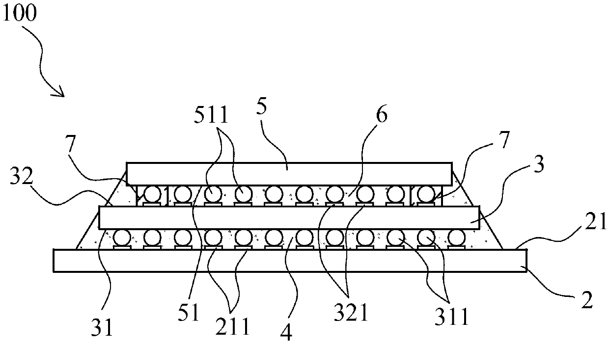
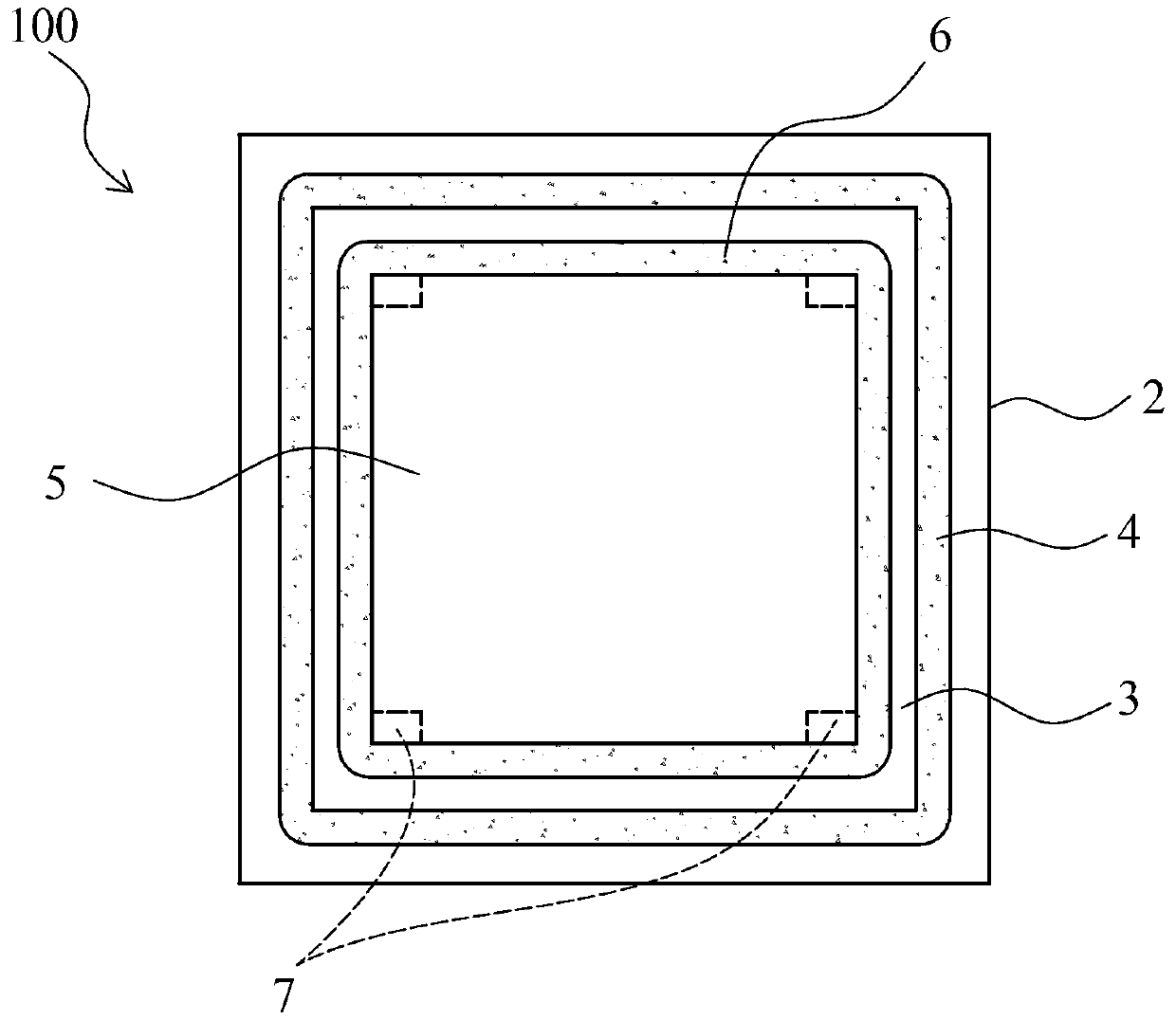
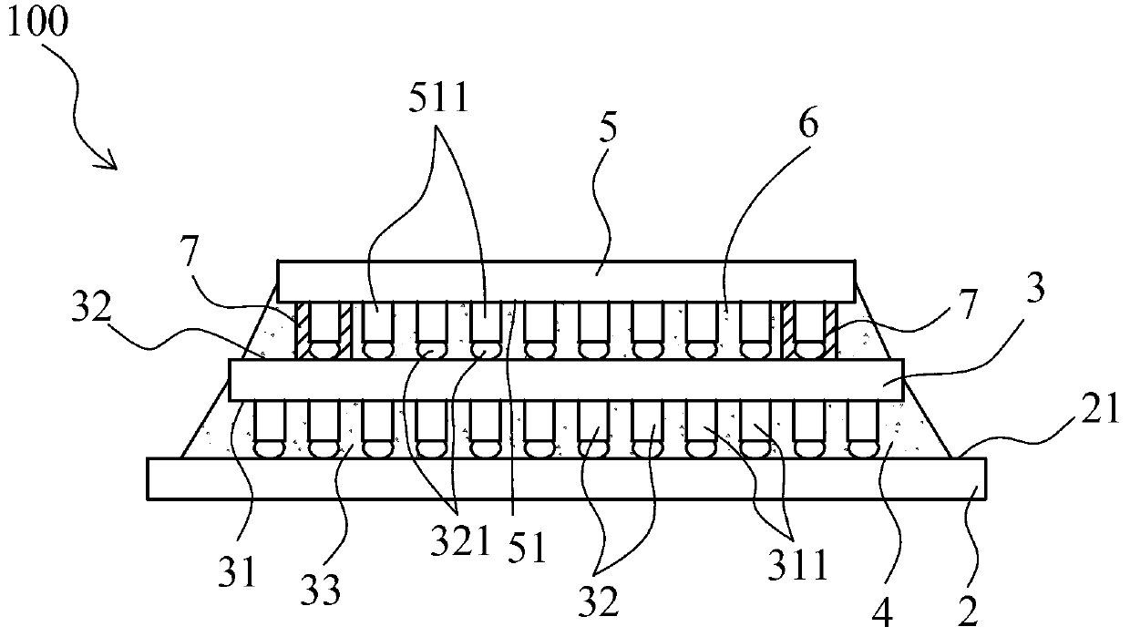
[0020] Please refer to Figure 1A , 1B As shown, the chip stacking structure 100 of an embodiment of the present invention mainly includes a substrate 2, a lower chip 3, a lower underfill 4 (underfill), an upper chip 5, an upper underfill 6 (underfill) and several The first bonding rubber block 7 . The ...


PUM


Abstract

The invention discloses a crystal plate stacked structure and a manufacturing method of the crystal plate stacked structure. The crystal plate stacked structure comprises a base plate, a lower crystal plate, lower bottom portion filling glue, an upper crystal plate, upper bottom portion filling glue and a plurality of first joint glue blocks. The first joint glue blocks are arranged between the lower crystal plate and the upper crystal plate and on a plurality of corner positions of the upper crystal plate, and are respectively connected with the lower crystal plate and the upper crystal plate. Due to the fact that the first joint glue blocks are respectively attached to the corner positions of the bottom face of the upper crystal plate, the first joint glue blocks are enabled to be fixedly connected with the upper crystal plate and the lower crystal plate by heating, therefore, in the process of filling the upper portion filling glue, the situation that contact is bad due to the fact that corners or edge of the upper crystal plate are warped is avoided.

Description

technical field [0001] The present invention relates to a wafer stacking structure and its manufacturing method, in particular to a wafer stacking structure and its manufacturing method. Background technique [0002] Nowadays, semiconductor devices such as portable personal computers, smart phones, and digital cameras all have multi-functional and high-performance designs, and there is a trend towards thinner and smaller, so semiconductor packages are used in many electronic devices. It is becoming more and more common in the world, and the warpage problem is also increasing in the semiconductor packaging process. In the previous studies, the warpage of the packaging structure was mainly caused by the uneven warpage caused by the different thermal expansion coefficients of the materials, or the material characteristics of the curing shrinkage after baking. [0003] For example, in the manufacturing process of the existing packaging structure, a flip-chip chip is first cove...

Claims


Application Information

Patent Timeline
Patent Type & Authority Applications(China)
IPC IPC(8): H01L25/00H01L23/31H01L21/56
CPCH01L21/563H01L2224/16145H01L2224/32145H01L2224/32225H01L2224/73204H01L2225/06517H01L2225/06513H01L2225/06568H01L24/81H01L2224/10165H01L2224/1146H01L2224/1147H01L2224/11849H01L2224/13082H01L2224/13111H01L2224/1319H01L2224/16227H01L2224/81007H01L2224/8114H01L2224/81191H01L2224/81193H01L2224/81194H01L2224/81203H01L2224/8123H01L2224/81234H01L2224/81815H01L2224/8192H01L2224/83104H01L2224/81868H01L2224/81885H01L2224/131H01L2224/13147H01L2224/16225H01L2224/13H01L2224/16H01L2924/00H01L2924/00014H01L2924/0665H01L2924/014
Inventor 王琇如许哲铭唐和明
Owner ADVANCED SEMICON ENG INC
Why Eureka
Try Eureka