
Semiconductor device and operating method thereof

A technology for semiconductors and devices, applied in the field of internal voltage generating circuits, can solve the problems of reduced response speed of internal voltage generating circuits, increased current usage of semiconductor devices, and deterioration of semiconductor device performance.

Active Publication Date: 2013-06-19
SK HYNIX INC
View PDF5 Cites 6 Cited by
  • Summary
  • Abstract
  • Description
  • Claims
  • Application Information

AI Technical Summary

Problems solved by technology

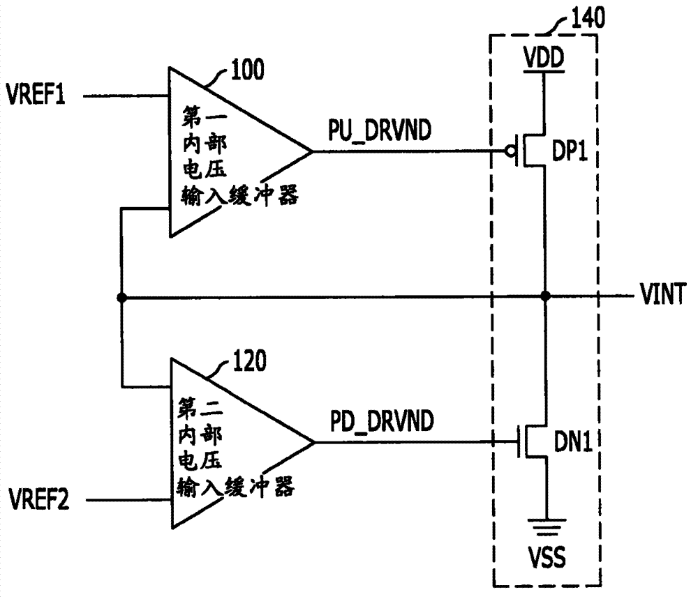
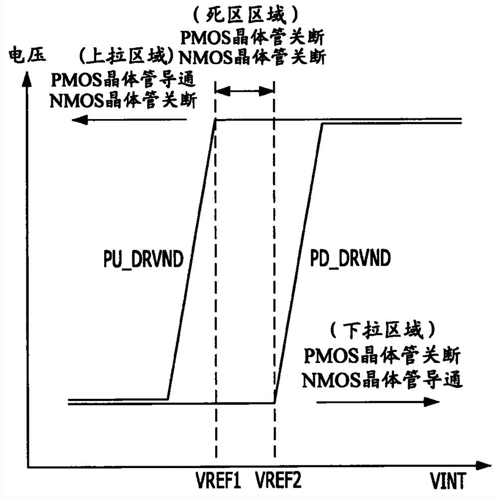
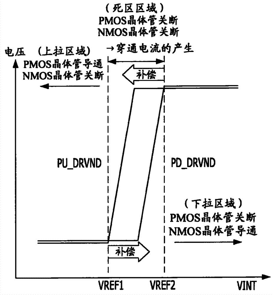
[0022] If the punch-through current phenomenon occurs in this way, the current usage of the semiconductor device suddenly increases, and thus, the power consumption of the semiconductor device increases, therefore, in the prior art, a dead zone equal to or greater than several tens of mV is maintained
[0023] Therefore, the reaction speed of the internal voltage generating circuit is basically lowered due to the existence of the dead area, and the performance of the semiconductor device may deteriorate

Method used


Image

  • Semiconductor device and operating method thereof
  • Semiconductor device and operating method thereof
  • Semiconductor device and operating method thereof

Examples


no. 1 example

[0037] Figure 3A with Figure 3B is a circuit diagram illustrating an internal voltage generating circuit of the semiconductor device according to the first embodiment of the present invention.

[0038] Figure 4 is description Figure 3A with Figure 3B A graph showing the operation of the internal voltage generating circuit of the semiconductor device according to the first embodiment of the present invention.

[0039] see Figure 3A , The internal voltage generating circuit of the semiconductor device according to the first embodiment of the present invention includes an internal voltage input buffer 300 , an internal voltage driving module 340 , a current supplying module 360 ​​and a current sinking module 370 . The internal voltage input buffer 300 includes a voltage detection unit 302 and a driving node level determination unit 304 . The driving node level determination unit 304 includes a supply current source 3042 , a sink current source 3044 and a floating curr...

no. 2 example

[0093] Figure 5A with Figure 5B is a circuit diagram illustrating an internal voltage generating circuit of a semiconductor device according to a second embodiment of the present invention.

[0094] Image 6 Is the explanation based on Figure 5A with Figure 5B A graph showing the operation of the internal voltage generating circuit of the semiconductor device of the second embodiment of the present invention.

[0095] see Figure 5A , the internal voltage generating circuit of the semiconductor device according to the second embodiment of the present invention includes a first internal voltage input buffer 500, a second internal voltage input buffer 560, a third internal voltage input buffer 570, and an internal voltage driving module 540A and 540B. The first internal voltage input buffer 500 includes a voltage detection unit 502 and a driving node level determination unit 504 . The driving node level determination unit 504 is configured to include a supply current ...


PUM


Abstract

The invention discloses a semiconductor device and operation methode for the same. The semiconductor device includes an internal voltage input buffer configured to determine voltage levels of a pull-up driving node and a pull-down driving node as a result of a comparison between a voltage level of an internal voltage node and a voltage level of a reference voltage node such that the pull-up driving node and the pull-down driving node to maintain a voltage level difference, and an internal voltage driving block configured to pull-up drive the internal voltage node in response to the voltage level of the pull-up driving node and pull-down drive the internal voltage node in response to the voltage level of the pull-down driving node.

Description

[0001] Cross References to Related Applications [0002] This application claims priority from Korean Patent Application No. 10-2011-0130951 filed on December 8, 2011, the entire contents of which are hereby incorporated by reference. technical field [0003] Exemplary embodiments of the present invention relate to a semiconductor design technology, to an internal voltage generating circuit of a semiconductor device and an operating method thereof, and more particularly, to a semiconductor device not including a dead zone operating region Internal voltage generating circuit and method of operation thereof. Background technique [0004] As critical dimensions and cell sizes of semiconductor devices decrease, supply voltages are also reduced, and therefore, design techniques for low voltage environments are useful. [0005] For example, a semiconductor device includes an internal voltage generating circuit that receives a power supply voltage (VDD) and generates an internal v...

Claims


Application Information

Patent Timeline
Patent Type & Authority Applications(China)
IPC IPC(8): G11C11/4074
CPCG11C5/147G11C5/14G11C7/10
Inventor 李俊揆
Owner SK HYNIX INC
Features
  • Generate Ideas
  • Intellectual Property
  • Life Sciences
  • Materials
  • Tech Scout
  • Unparalleled Data Quality
  • Higher Quality Content
  • 60% Fewer Hallucinations
Learn More