Support plate for failure analysis, test equipment, and method for chip electrical failure analysis

A technology for electrical failure and testing equipment, which is applied in electronic circuit testing, optical testing for flaws/defects, measuring device casings, etc. It can solve problems such as inability to successfully solder all of them, inability to handle chips with a large number of pins, and complex pin arrangement. , to achieve the effect of convenient and fast hardware preparation

Active Publication Date: 2013-07-03
SEMICON MFG INT (SHANGHAI) CORP
View PDF4 Cites 21 Cited by
  • Summary
  • Abstract
  • Description
  • Claims
  • Application Information

AI Technical Summary

Problems solved by technology

Such a method cannot handle chips with a large number of pins, because there are too many pins, the success rate of welding is very low, or the pin arrangement is complicated, so all of them cannot be successfully soldered.

Method used


Image

  • Support plate for failure analysis, test equipment, and method for chip electrical failure analysis
  • Support plate for failure analysis, test equipment, and method for chip electrical failure analysis
  • Support plate for failure analysis, test equipment, and method for chip electrical failure analysis

Examples


specific example

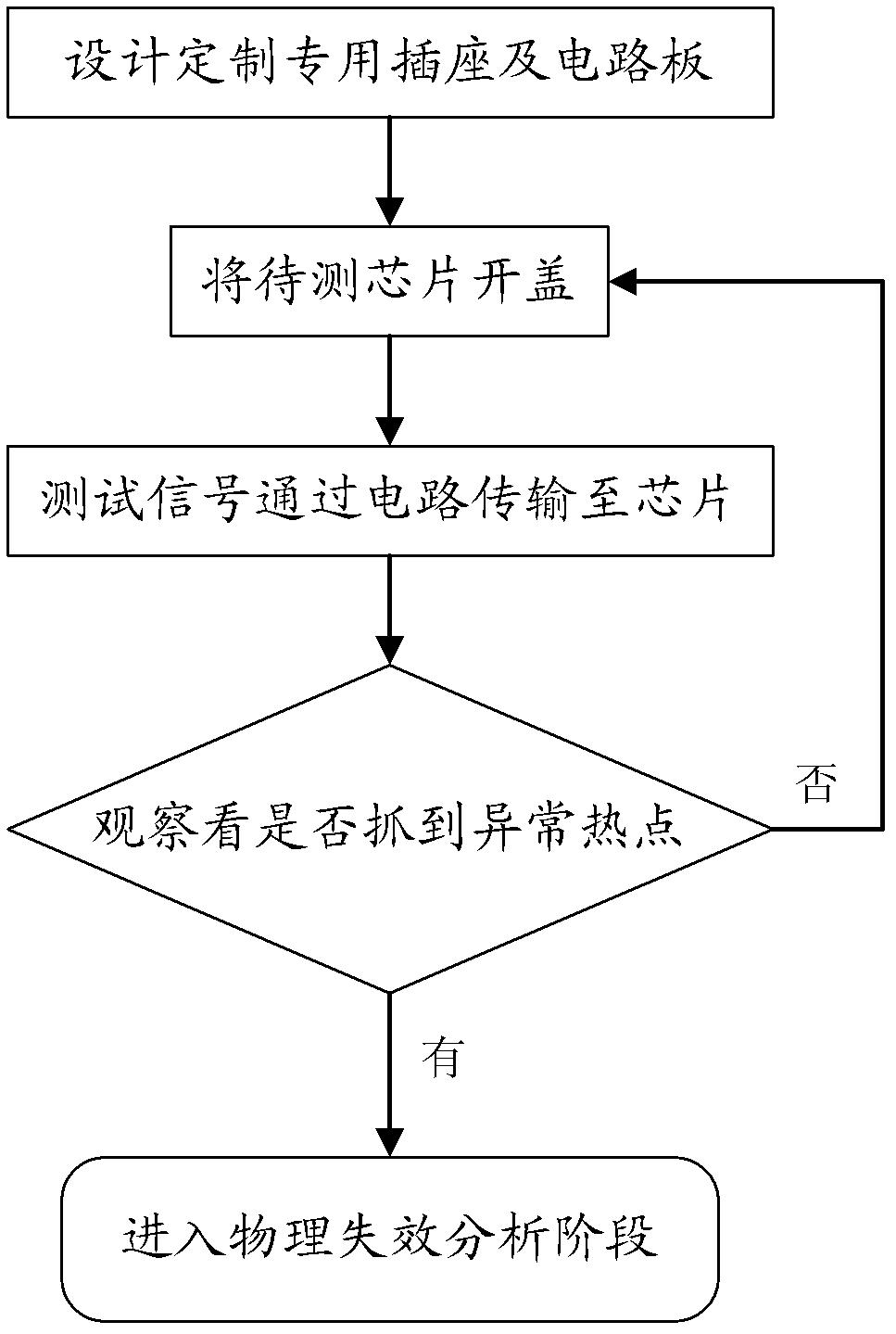
[0063] The following is a specific example, combined with Figure 6 to Figure 8 To describe in detail the method of using the present invention to test the special-purpose carrier board designed for the chip to be tested:

[0064] 1) Design a special carrier board for the chip to be tested;

[0065] The chip to be tested is a 360-pin BGA with a pin center distance of 1.5 mm, which is only 31 mm square. Ten chips are randomly selected from a certain batch of chips that have problems and need to be analyzed for failure as test samples, which are the chips to be tested in this embodiment.

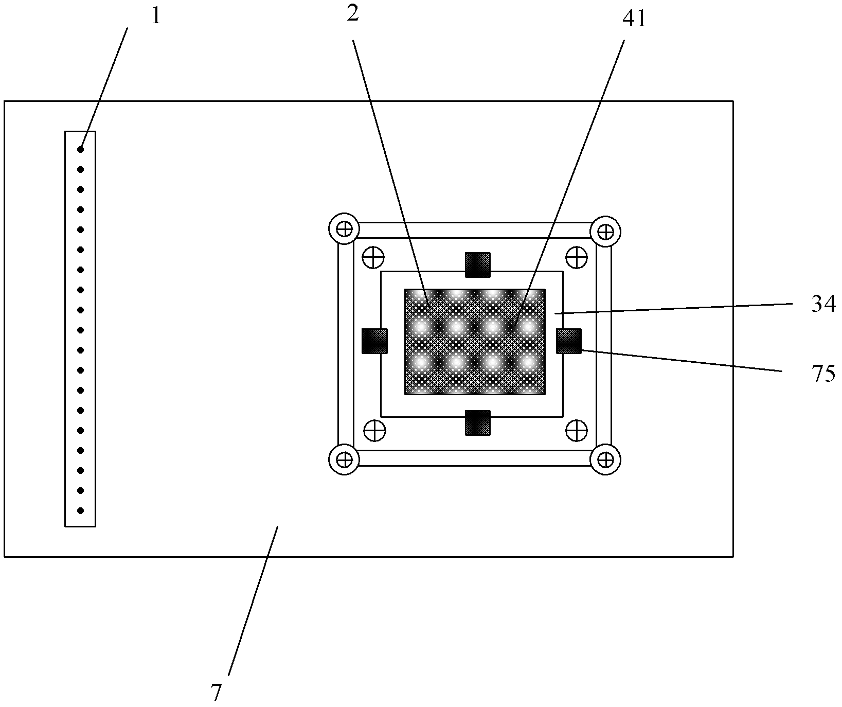
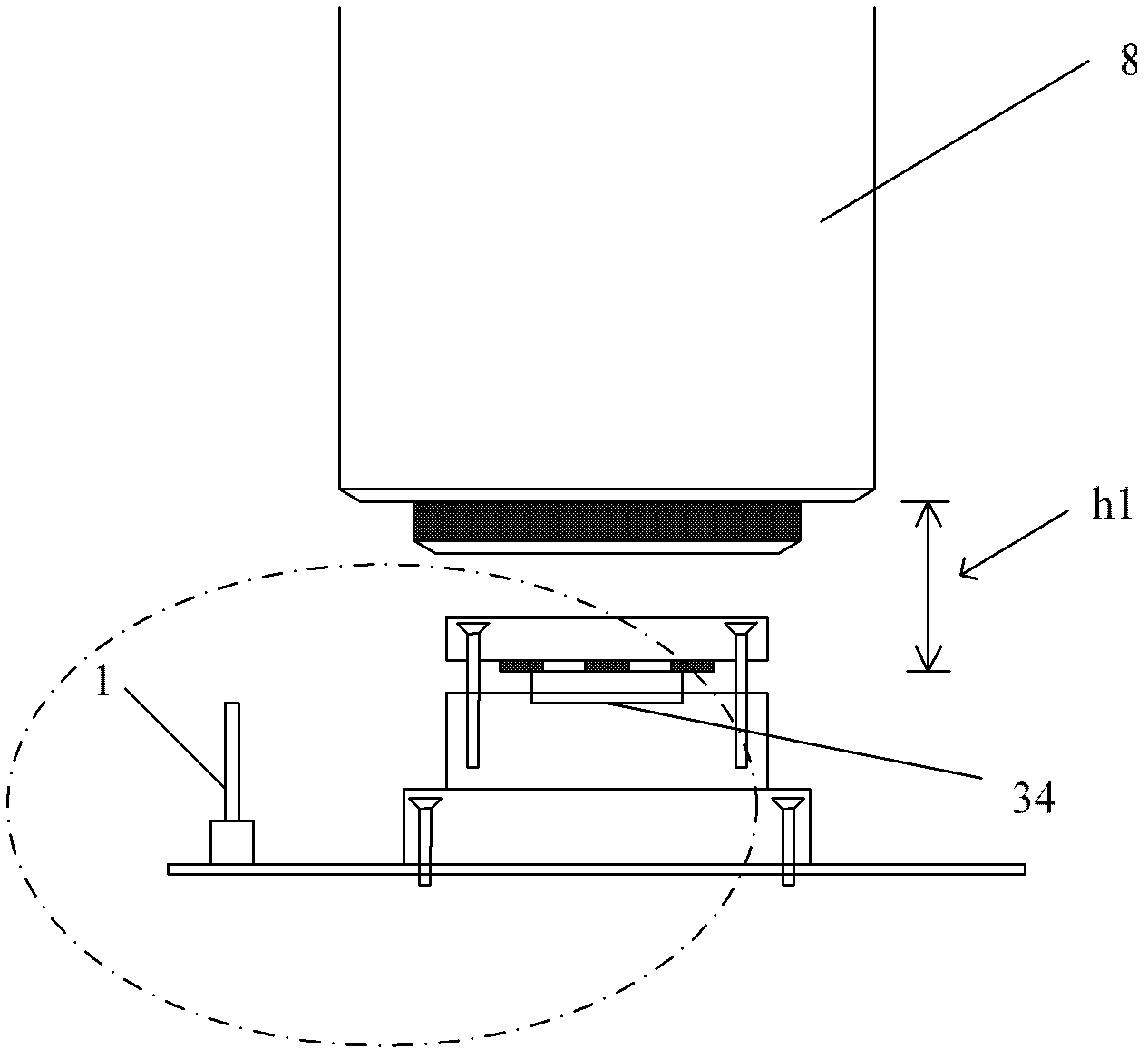
[0066] The carrier board, which is a PCB board, includes an array of pins for signal transmission between the chip and the test machine, an array of pads in the area where the chip to be tested is set, and a gap between the array of pins and the array of pads. Metal connection. The pins are generally copper pillars, and their number is compatible with the input and output pins of the chip. ...


PUM

PropertyMeasurementUnit
thicknessaaaaaaaaaa
thicknessaaaaaaaaaa

Abstract

The invention provides a support plate specially designed for a chip to be tested, test equipment, and a method for chip electrical failure analysis. According to the method, the support plate is specially designed for the chip to be tested, wherein the support plate comprises a pad array located in a containing area of the chip to be tested, a pin array used for realizing signal transmission with a test machine, and metal cables used for connecting the pin array and the pad array, and the chip to be tested is stuck to the support plate with the surface mounted technology (SMT). According to the method for the chip electrical failure analysis, the support plate used for the chip electrical failure analysis and the test equipment, hardware preparation can be achieved conveniently and fast, and the chip electrical failure analysis of tests of chips with a large amount of pins can be achieved easily.

Description

technical field [0001] The invention relates to the technical field of semiconductors, in particular to a detection device, equipment and method for chip electrical failure analysis. Background technique [0002] In the process of improving product yield, product engineers need to conduct electrical and physical failure analysis on problematic products, so as to diagnose the products. Through electrical failure analysis, it is often possible to find out the position of the defect on the layout. In order to clarify the specific situation of the defect, a physical failure analysis is required, mainly including delamination, focused ion beam (FIB), scanning electron microscope (SEM), Transmission electron microscopy (TEM), VC localization technique and defect chemical composition analysis. Electrical failure analysis is the premise of physical failure analysis, and the results of physical failure analysis are the purpose and evidence of electrical failure analysis. In failure...

Claims


Application Information

Patent Timeline
Patent Type & Authority Applications(China)
IPC IPC(8): G01R31/28G01R1/04G01N21/88
Inventor 熊晓东刘喆秋
Owner SEMICON MFG INT (SHANGHAI) CORP
Why Eureka
Try Eureka