Circuit and method for testing liquid crystal display device
A liquid crystal display device and testing circuit technology, which is applied in nonlinear optics, instruments, optics, etc., can solve the problems of production waste, inability to detect the short circuit phenomenon of the scanning electrode lines of the liquid crystal display device, etc., so as to improve the accuracy and avoid production. wasteful effect
- Summary
- Abstract
- Description
- Claims
- Application Information
AI Technical Summary
Problems solved by technology
Method used
Image
Examples
Embodiment 1
[0040] For ease of description, this embodiment will take a test circuit including two scan electrode test blocks as an example to describe the test circuit provided by the present invention, but it should be noted that, for the test circuit provided by the present invention The number is not limited in the present invention, as long as the test circuit includes at least two scan electrode test blocks, it belongs to the protection scope of the present invention.
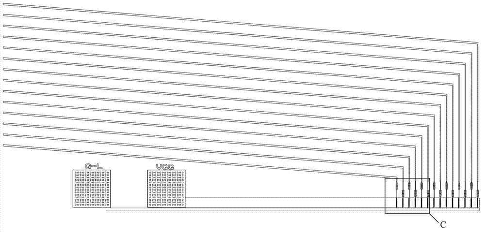
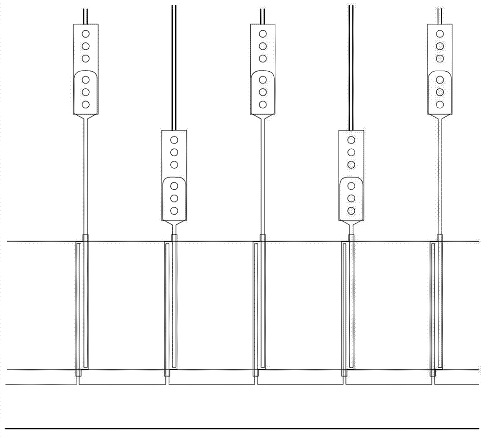
[0041] The test circuit of the liquid crystal display device provided by this embodiment, such as Figure 4 As shown, it includes: a first scan electrode test block 401 , a second scan electrode test block 402 and a plurality of scan electrode lines 403 . Wherein, adjacent scan electrode lines of the plurality of scan electrode lines 403 are electrically connected to the first scan electrode test block 401 and the second scan electrode test block 402 respectively.
[0042] When the scanning electrode line of the liq...
Embodiment 2
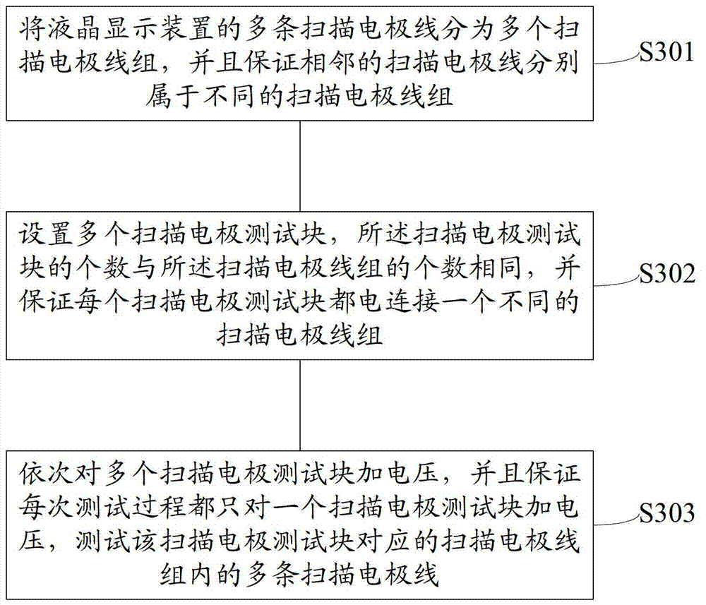
[0048] This embodiment provides a liquid crystal display device testing method, comprising the following steps:
[0049] Step S301: Divide multiple scan electrode lines of the liquid crystal display device into multiple scan electrode line groups, and ensure that adjacent scan electrode lines belong to different scan electrode line groups.
[0050] In this embodiment, a plurality of scanning electrode lines of a liquid crystal display device are divided into two groups as an example for illustration. Divide multiple scan electrode lines into the first scan electrode line group and the second scan electrode line group, and ensure that adjacent scan electrode lines are in different scan electrode line groups, that is, belong to the first scan electrode line group and the second scan electrode line group The scanning electrode lines of the second scanning electrode line group are arranged at intervals, and there is a scanning electrode line belonging to the second scanning electr...
PUM
 Abstract
Description
Claims
Application Information


