Source follower based on deep n-well nmos transistor

A technology of source follower and transistor, which is applied in the direction of logic circuit coupling/interface, logic circuit connection/interface layout, etc. using field effect transistors, which can solve problems such as dynamic distortion and high-frequency dynamic distortion performance without consideration, and achieve dynamic Small distortion, reduced parasitic capacitance, and the effect of solving dynamic distortion

Inactive Publication Date: 2016-05-11
芯锋宽泰科技(北京)有限公司
View PDF5 Cites 0 Cited by
  • Summary
  • Abstract
  • Description
  • Claims
  • Application Information

AI Technical Summary

Problems solved by technology

[0010] To avoid the linear distortion caused by the voltage-dependent body effect, a source follower based on a deep N-well NMOS transistor was further proposed, but this source follower did not consider the parasitic capacitance in the deep N-well NMOS transistor at high frequency The impact on its high-frequency dynamic distortion performance during application, usually, dynamic distortion is prone to occur in high-frequency or high-speed applications

Method used


Image

  • Source follower based on deep n-well nmos transistor
  • Source follower based on deep n-well nmos transistor
  • Source follower based on deep n-well nmos transistor

Examples


Embodiment Construction

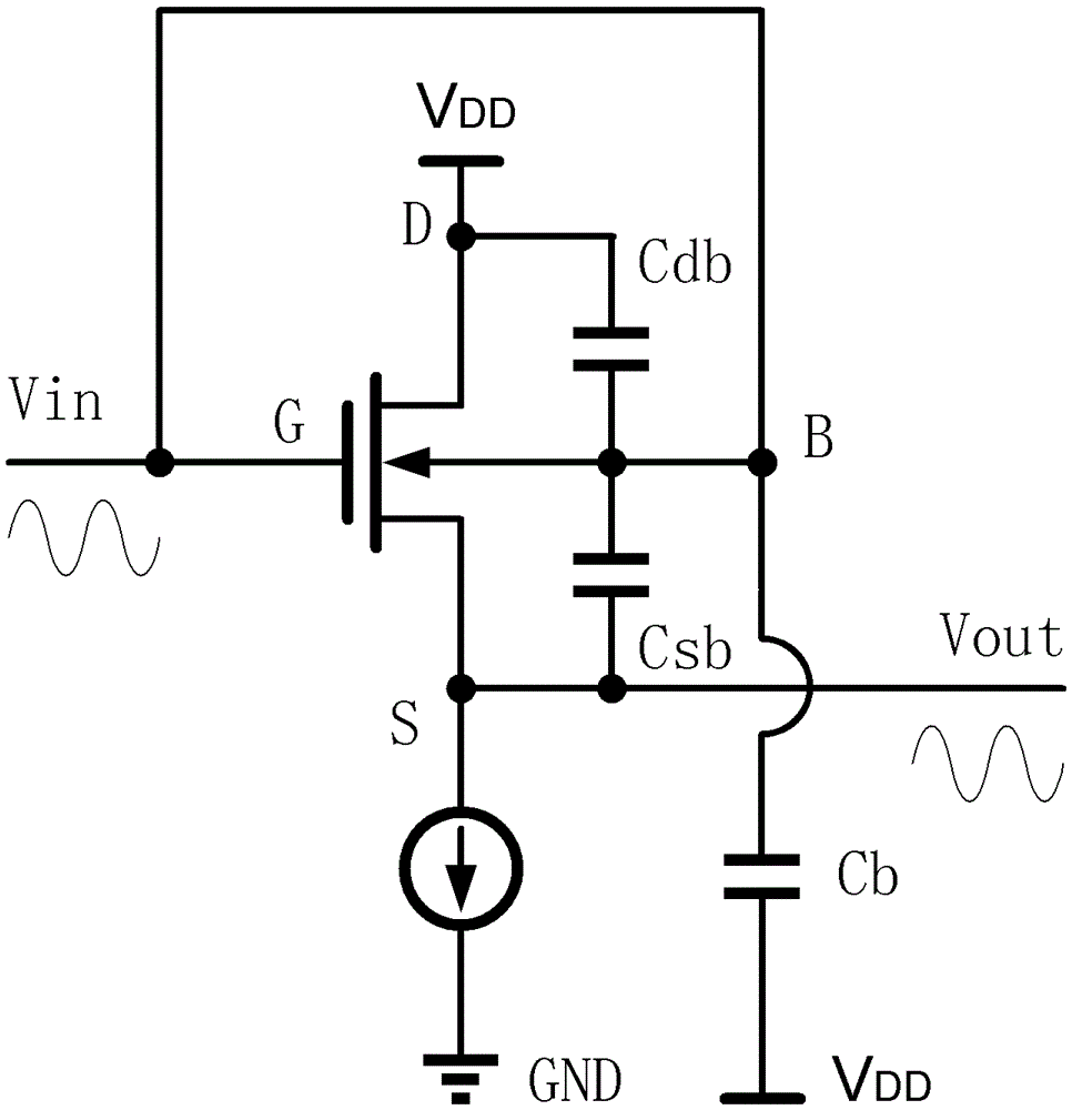
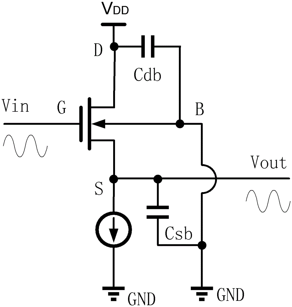
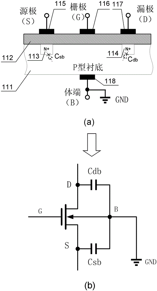
[0037] The following introduces some of the possible embodiments of the present invention, which are intended to provide a basic understanding of the present invention, but are not intended to identify key or decisive elements of the present invention or limit the scope of protection. It is easy to understand that, according to the technical solution of the present invention, those skilled in the art may propose other alternative implementation manners without changing the essence and spirit of the present invention. Therefore, the following specific embodiments and drawings are only exemplary descriptions of the technical solution of the present invention, and should not be regarded as the entirety of the present invention or as a limitation or restriction on the technical solution of the present invention.

[0038] It will be understood that when a component is referred to as being "connected" to another component, it can be directly connected to the other component or interv...


PUM


Abstract

The invention provides a source electrode follower based on a deep N-well N-channel metal oxide semiconductor (NMOS) transistor, and belongs to the technical filed of source followers. The source electrode follower comprises a current source and the deep N-well NMOS transistor which is used as an input component, wherein a body end of the deep N-well NMOS transistor is connected with an input end (Vin) of the source electrode follower, and so that a voltage (Vsb) between a source electrode of the deep N-well NMOS transistor and the body end of the deep N-well NMOS transistor is basically maintained to be constant under the situation that an input signal is changed. The source electrode follower based on the deep N-well NMOS transistor is small in distortion, good in linearity, and particularly suitable for the application in high-speed heavy load occasions.

Description

technical field [0001] The invention belongs to the field of source follower technology, and relates to a source follower based on a deep N-well NMOS transistor. Background technique [0002] Source followers based on MOS devices (that is, MOSFETs, that is, MOS transistors) are widely used in various functional circuits. For example, the source follower can usually be used as a high-speed input buffer, its circuit structure is simple, the source follower can provide high input impedance, low output impedance and wide signal bandwidth; compared with the operational amplifier based on closed-loop drive, the source follower There are no stability issues with the device. Therefore, source followers are well suited for buffer and driver circuits. [0003] figure 1 Shown is a schematic diagram of a standard NMOS transistor, where (a) is a schematic diagram of its cross-sectional structure, and (b) is a schematic diagram of its equivalent circuit. figure 2 shown based on figu...

Claims


Application Information

Patent Timeline
Patent Type & Authority Patents(China)
IPC IPC(8): H03K19/0185
Inventor 刘松杨飞琴吴柯
Owner 芯锋宽泰科技(北京)有限公司
Why Eureka
Try Eureka