Manufacture method of thick copper plate fine solder resist bridge

A manufacturing method and technology of solder mask bridges, which are applied in printed circuit manufacturing, electrical components, printed circuits, etc., can solve the problems of low efficiency, low yield, and poor product appearance of fine green oil bridges, so as to avoid appearance defects, Effects that satisfy the thickness condition

Inactive Publication Date: 2013-07-10
SHENZHEN KINWONG ELECTRONICS
View PDF6 Cites 24 Cited by
  • Summary
  • Abstract
  • Description
  • Claims
  • Application Information

AI Technical Summary

Problems solved by technology

[0005] In view of the above-mentioned deficiencies in the prior art, the purpose of the present invention is to provide a method for manufacturing fine solder-resist bridges on thick copper plates, aiming to solve the problems of low efficiency in making fine green oil bridges, poor product appearance, and low yield rate

Method used


Image

  • Manufacture method of thick copper plate fine solder resist bridge
  • Manufacture method of thick copper plate fine solder resist bridge

Examples


Embodiment Construction

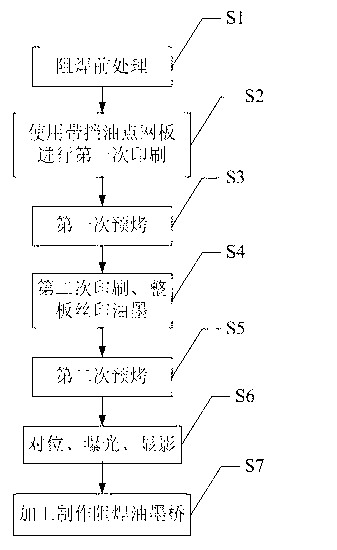
[0019] The present invention provides a method for manufacturing a fine solder-resisting bridge of thick copper plate. In order to make the purpose, technical solution and effect of the present invention clearer and clearer, the present invention will be further described in detail below. It should be understood that the specific embodiments described here are only used to explain the present invention, not to limit the present invention.

[0020] A method for manufacturing fine solder-resisting bridges for thick copper plates of the present invention is used for processing thick copper plates with a thickness ≥ 2 OZ, and the width of the processed solder-resisting ink bridges is ≤ 4 mils. Solder-resist bridges less than 4mil often cause processing quality degradation due to side erosion during printing ink, and this method can avoid the occurrence of this problem. The method adopted by this method includes the following steps: use oil-repelling points for thick copper circuit ...


PUM


Abstract

The invention discloses a manufacture method of a thick copper plate fine solder resist bridge. The manufacture method comprises the following steps of: baffling printing ink at the position of a fine solder resist bridge by a mesh plate with oil baffle points when first oil printing is carried out, wherein the thickness of the printing ink of a thick copper plate line can be guaranteed only by printing the printing ink at the other positions; and carrying out second printing by a normal blank mesh plate. After the method is used, under the condition that the thickness of the printing ink of the thick copper plate line is guaranteed, the thickness of the printing ink at the fine solder resist bridge is reduced, and the thickness condition of the manufactured fine solder resist bridge can be met; the conventional double-alignment, exposure and development technology is changed into one-time-alignment, exposure and development technology after the whole craft process is used; and the printing oil at the edge within an oil baffle region inwards leaks due to the liquidity of the printing ink after the first printing, so that the stepped drop can be avoided in the process of secondary silk screen, and the thick copper plate fine solder resist bridge is attractive in appearance. The stepped apparent defect caused by the double times of exposure and development can be avoided.

Description

technical field [0001] The invention relates to the technical field of PCB manufacturing, in particular to a method for manufacturing a fine solder-resisting bridge of a thick copper plate. Background technique [0002] In order to ensure the thickness of ink on the circuit when making solder resist on thick copper plate (≥2OZ), it is often made by two printings or multiple printings, but after printing, the ink will be thicker due to the position of the substrate (generally equivalent to the thickness of copper, that is, ≥ 70um), when making small green oil bridges, due to side erosion, the quality of the green oil bridges is often abnormal, which seriously troubles the industry to mass-produce such products. [0003] At present, for this type of board, circuit board manufacturers generally use two printings, two alignments, exposure and development: Method 1. Make the green oil bridge in the first printing and alignment exposure development, and the second alignment Open ...

Claims


Application Information

Patent Timeline
Patent Type & Authority Applications(China)
IPC IPC(8): H05K3/00
Inventor 陈晓宇游俊
Owner SHENZHEN KINWONG ELECTRONICS
Why Eureka
Try Eureka