Clean room for semiconductor plant

A semiconductor and clean room technology, applied in the field of clean rooms, can solve the problems of hindering personnel movement, difficult to grasp the distance, time-consuming and laborious, etc., to avoid the impact of storage bins and products, facilitate construction, and reduce costs.

Active Publication Date: 2013-07-17
L&K ENG SUZHOU
View PDF4 Cites 3 Cited by
  • Summary
  • Abstract
  • Description
  • Claims
  • Application Information

AI Technical Summary

Problems solved by technology

[0007] However, the above-mentioned technical solution has the following problems: (1) Since partitions are arranged around the production aisle, and there is a gap between the partitions and the placement area directly below them, the air damper is formed, that is, the partitions and the directly below The distance between the placement areas is very small, therefore, the partition separates the production aisle from the service area, hindering the movement of personnel; (2) due to the need to form gas between the partiti

Method used


Image

  • Clean room for semiconductor plant
  • Clean room for semiconductor plant
  • Clean room for semiconductor plant

Examples


Embodiment 1

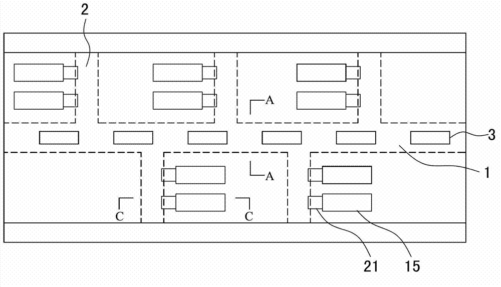
[0041] see Figure 4~6 As shown, a clean room for a semiconductor plant, including a fresh air delivery system, an exhaust system and a large clean space, the large clean space has a central aisle 1 and 5 production aisles 2;

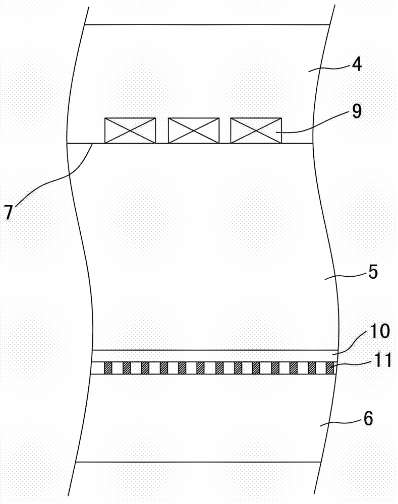
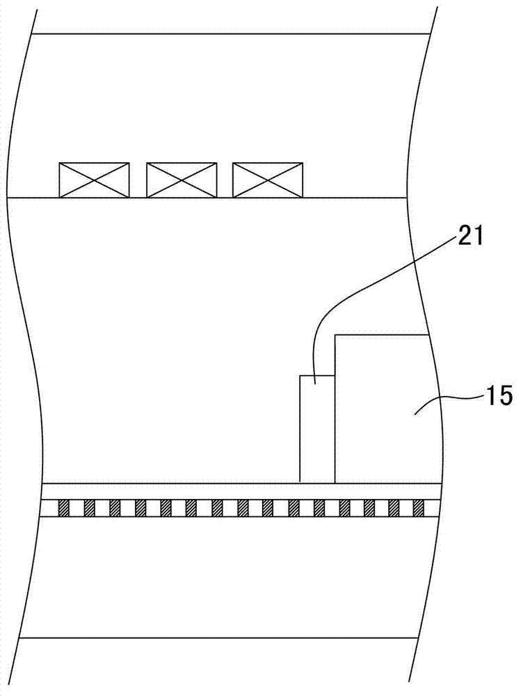
[0042] The large clean space includes a structure space 4, a clean space 5 and a circulation space 6 from top to bottom, a ceiling 7 is provided between the structure space and the clean space, and a raised floor 10 and a concrete slab 11 are provided between the clean space and the circulation space ;

[0043] Partitions 8 are arranged around the production walkway, so that at least a part of the architectural space, the clean space, and the space where the raised floor is located form an independent clean micro-environment structure; the distance between the bottom of the partition and the ceiling is 60cm, and the distance between the bottom of the partition and the raised floor is 2m;

[0044] The top of the clean microenvironment is provided with ...


PUM


Abstract

The invention discloses a clean room for semiconductor plant. The clean room comprises a new wind conveying system, an exhausting system and a large clean space. The large clean space has a central aisle and at least a production aisle, wherein a clapboard is arranged around the production aisle, so that at least a part of the frame space, the clean space and the space where a raised floor locates form an independent clean micro-environmental structure. The distance between the bottom of the clapboard and the ceiling is at least 60 cm, and the distance between the bottom of the clapboard and the raised floor is at least 2m. An upper seal plate and a lower sealplate are respectively arranged on the top and the bottom of the clean micro-environment, and the breadth of the lower sealplate is smaller than the breadth of the upper sealplate. According to the clean room, the clapboards are arranged around the production aisle to form an independent clean micro-environmental structure, so that the effects on the storage and the products of the central aisle and the production aisle due to the corrosive gas are avoided.

Description

technical field [0001] The invention relates to a clean room used in a semiconductor workshop, in particular to a production occasion for high-end semiconductors. Background technique [0002] The semiconductor plant is a place specially used to prepare semiconductor devices, and it has been widely used at present. Due to the particularity of semiconductor devices, semiconductor plants must be designed as clean rooms to meet the requirements of constant temperature, humidity and cleanliness. For some high-end semiconductor production plants, such as 32 / 28nm and even below high-end processes, not only have higher requirements for cleanliness, but also have stricter pollution of suspended chemical molecules floating in the air. [0003] Existing cleanrooms for semiconductor fabs see attached Figure 1~3 As shown, it mainly includes a fresh air conveying system, an exhaust system and a large clean space in which various processing equipment are arranged, and a central corridor...

Claims


Application Information

Patent Timeline
IPC IPC(8): E04H5/02E04H1/12
Inventor 杨政谕
Owner L&K ENG SUZHOU
Why Eureka
Try Eureka