Supercharge Your Innovation With Domain-Expert AI Agents!

Array substrate, manufacturing method thereof, and display device

The technology of an array substrate and its manufacturing method is applied in the field of array substrate and its manufacturing method and display device, and can solve the problems that liquid crystal displays cannot automatically adjust the display brightness according to the intensity of light.

Active Publication Date: 2015-10-14
BEIJING BOE OPTOELECTRONCIS TECH CO LTD
View PDF6 Cites 0 Cited by
  • Summary
  • Abstract
  • Description
  • Claims
  • Application Information

AI Technical Summary

Problems solved by technology

[0006] Embodiments of the present invention provide an array substrate and its manufacturing method and display device, which are used to solve the problem that the liquid crystal display in the prior art cannot automatically adjust its display brightness according to the intensity of light in the external environment

Method used


Image

  • Array substrate, manufacturing method thereof, and display device
  • Array substrate, manufacturing method thereof, and display device
  • Array substrate, manufacturing method thereof, and display device

Examples


Embodiment Construction
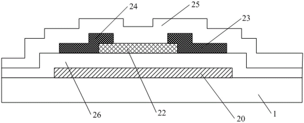
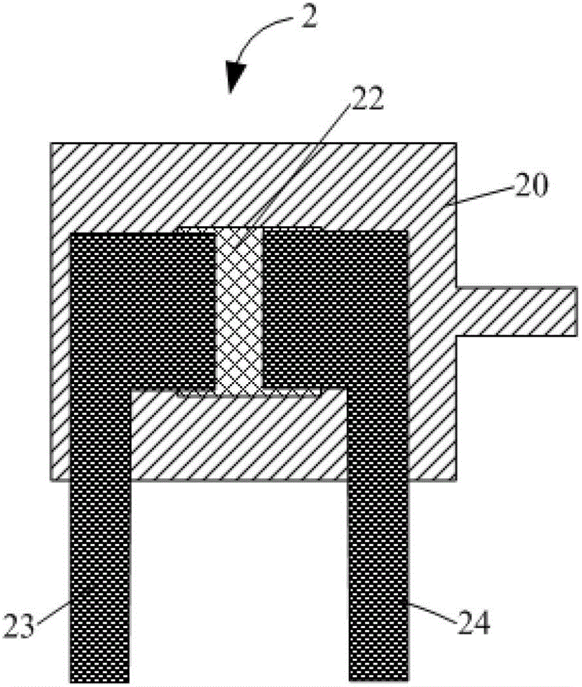
[0041] The non-display area of ​​the array substrate in the embodiment of the present invention includes at least one photosensitive sensor, and the amorphous silicon in the amorphous silicon layer of the photosensitive sensor can generate photocarriers under the condition of light, and the external light The stronger it is, the larger the photogenerated carriers will be. Connect the output electrode of the photosensitive sensor with the photoelectric detection circuit, so that the intensity of the external light can be detected in real time through the photosensitive sensor and the photoelectric detection circuit, and according to the external light Adjust the brightness of the backlight by strength or weakness.

[0042] The embodiments of the present invention will be further described in detail below in conjunction with the accompanying drawings.

[0043] The array substrate in the embodiment of the present invention includes a display area and a non-display area, wherein t...


PUM

PropertyMeasurementUnit
thicknessaaaaaaaaaa

Abstract

An array substrate, a manufacturing method thereof, and a display device are provided. The array substrate includes a display area and a non-display area. The non-display area includes at least one light sensor each including a light blocking layer on a substrate and for blocking light emitted from a backlight source; an insulating layer on the light blocking layer; a amorphous silicon layer on the insulating layer at a location corresponding to the light blocking layer and for sensing external light; an input electrode and an output electrode on the amorphous silicon layer and not contacting each other. The input electrode and the output electrode both contact the amorphous silicon layer, a part of the amorphous silicon layer between the input electrode and the output electrode forms a conductive channel. The output electrode is connected with a photoelectric detection circuit for inputting drain current generated by the conductive channel into the photoelectric detection circuit.

Description

technical field [0001] The invention relates to the field of liquid crystal display, in particular to an array substrate, a manufacturing method thereof, and a display device. Background technique [0002] Due to the characteristics of low radiation, light volume, small weight and low power consumption, liquid crystal displays (Liquid Crystal Display, LCD) have gradually replaced traditional cathode ray tube (Cathode Ray Tube, CRT) displays and are widely used in desktop computers. , notebook computers, personal digital assistants (Personal Digital Assistant, PDA), mobile phones, televisions and other fields. [0003] The existing liquid crystal display mainly includes a liquid crystal module and a backlight module. Since the liquid crystal itself does not emit light, it needs to rely on the backlight module inside the liquid crystal display to provide a backlight for it. The backlight module passes the light emitted by the backlight through the optical structure. The film ...

Claims


Application Information

Patent Timeline
Patent Type & Authority Patents(China)
IPC IPC(8): G02F1/1362G02F1/1368G02F1/1333
CPCH01L27/1443G02F1/13318G02F1/133512G02F2001/133388H01L27/1446H01L31/0203H01L31/02164H01L31/202H01L29/78633H01L29/78678G02F1/133388
Inventor 谢振宇徐少颖李田生阎长江
Owner BEIJING BOE OPTOELECTRONCIS TECH CO LTD
Features
  • R&D
  • Intellectual Property
  • Life Sciences
  • Materials
  • Tech Scout
  • Unparalleled Data Quality
  • Higher Quality Content
  • 60% Fewer Hallucinations
Learn More