Thickness and planeness measuring method for surface mounting technology (SMT) screen
A measurement method and flatness technology, which is applied in the field of SMT stencil thickness and flatness measurement, can solve the problems of not being able to express the thickness of a specific area and measuring the thickness of the stencil, and achieve improved measurement accuracy, reduced errors, and good technical effects Effect
- Summary
- Abstract
- Description
- Claims
- Application Information
AI Technical Summary
Problems solved by technology
Method used
Image


Examples
Embodiment 1
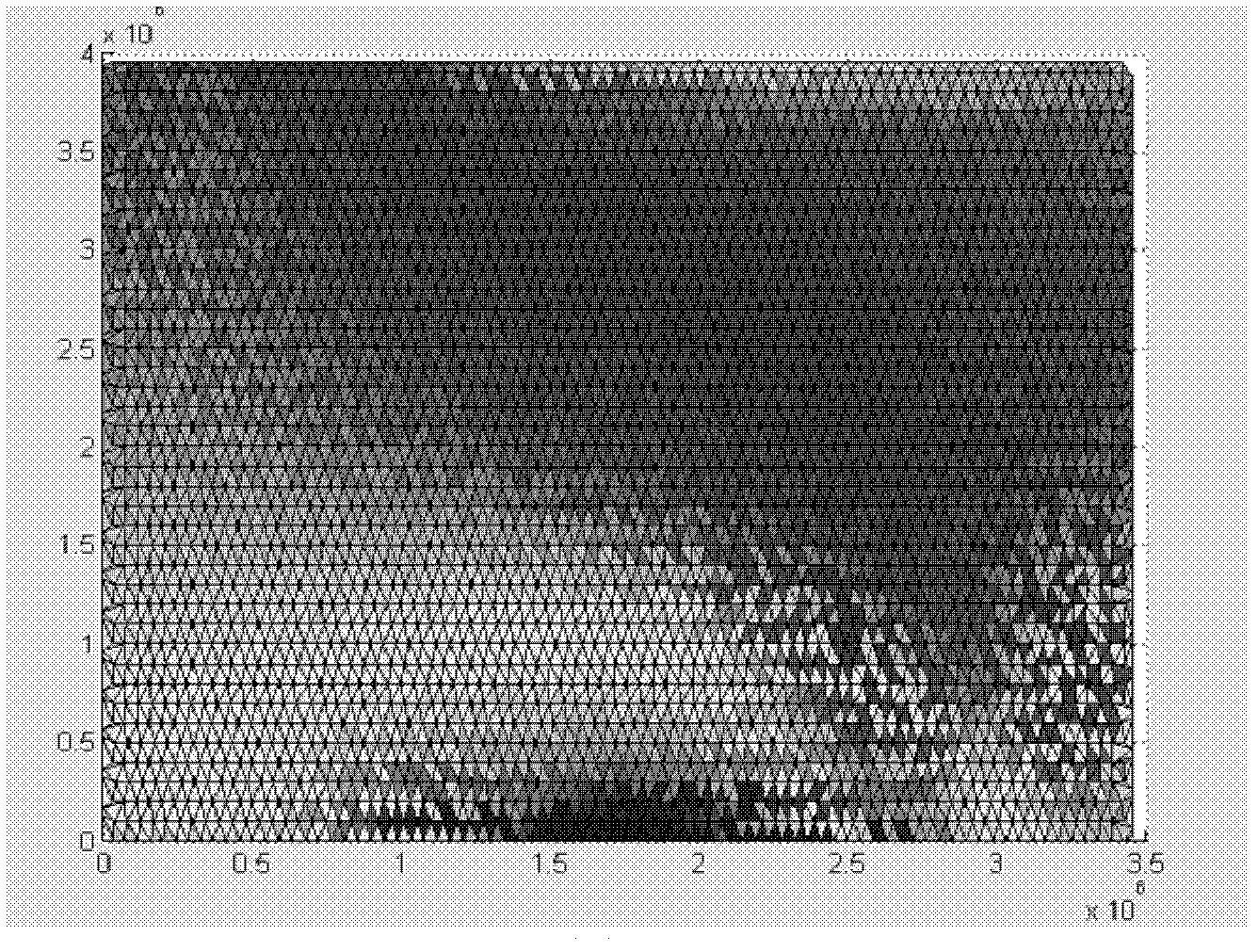
[0022] A method for measuring the thickness and flatness of an SMT stencil, comprising the following steps: using a standard block to calibrate to determine the distance between two sensors; laying the stencil flat, moving it through a shaft system, and moving the two coaxial The laser displacement sensor moves to the starting position of the lower left corner of the screen; use the laser displacement sensor to move along a certain path to complete the scanning of the entire format of the screen, and collect the distance information between the upper and lower surfaces and each sensor; after scanning, according to The coordinates of the points and the obtained thickness information, the obtained distance between the upper and lower surfaces and the sensor and their coordinates are fitted into a thickness distribution diagram and a fitted surface diagram of the upper and lower surfaces.
[0023]
Embodiment 2
[0025] A method for measuring the thickness and flatness of an SMT stencil, which uses two coaxial laser displacement sensors to scan the entire format of the stencil and collect the distance information between the upper and lower surfaces and each sensor. After the scanning is completed, the obtained upper and lower The distance between the surface and the sensor and its coordinates are fitted into a thickness distribution map and a fitting surface map of the upper and lower surfaces. At the beginning, use the standard block to calibrate, determine the distance between the two sensors, place the stencil, and move the laser displacement sensor to the starting position of the lower left corner of the stencil by moving the shaft system, and then start to acquire thickness data and move along the figure 2 The path shown is moved to complete the scanning of the entire web of the stencil. The length interval of the thickness data collection during scanning can be set, and the thi...
Embodiment 3
[0028] SMT stencil thickness and flatness measurement method, including the following steps: use the standard block calibration to determine the distance between the two sensors; lay the stencil flat, move through the shaft system, and displace the two coaxial lasers The sensor moves to the starting position in the lower left corner of the screen; c) Use the laser displacement sensor to move along a certain path to complete the scanning of the entire format of the screen, and collect the distance information between the upper and lower surfaces and each sensor; d) After the scanning is completed , according to the coordinates of the points and the obtained thickness information, the obtained distance and coordinates between the upper and lower surfaces and the sensor are fitted into a thickness distribution diagram and a fitted surface diagram of the upper and lower surfaces. Set the length interval of the thickness data collection during scanning, and collect and save the thic...
PUM
 Abstract
Description
Claims
Application Information
 - R&D
- Intellectual Property
- Life Sciences
- Materials
- Tech Scout
- Unparalleled Data Quality
- Higher Quality Content
- 60% Fewer Hallucinations
Browse by: Latest US Patents, China's latest patents, Technical Efficacy Thesaurus, Application Domain, Technology Topic, Popular Technical Reports.
© 2025 PatSnap. All rights reserved.Legal|Privacy policy|Modern Slavery Act Transparency Statement|Sitemap|About US| Contact US: help@patsnap.com