TFT (thin film transistor) threshold voltage compensation method, TFT (thin film transistor) threshold voltage compensation circuit, shift register and display device

A shift register and compensation circuit technology, applied in static memory, digital memory information, instruments, etc., can solve problems such as inconsistent threshold voltage, failure to work, and offset

Active Publication Date: 2013-07-24
BOE TECH GRP CO LTD
View PDF3 Cites 6 Cited by
  • Summary
  • Abstract
  • Description
  • Claims
  • Application Information

AI Technical Summary

Problems solved by technology

[0007] Embodiments of the present invention provide a TFT threshold voltage offset compensation circuit and method, a shift register, and a display device, which are used to solve the problem of inconsistency or offset of the current threshold voltage of the thin film transistor at the output end in the existing shift register. work problem

Method used


Image

  • TFT (thin film transistor) threshold voltage compensation method, TFT (thin film transistor) threshold voltage compensation circuit, shift register and display device
  • TFT (thin film transistor) threshold voltage compensation method, TFT (thin film transistor) threshold voltage compensation circuit, shift register and display device
  • TFT (thin film transistor) threshold voltage compensation method, TFT (thin film transistor) threshold voltage compensation circuit, shift register and display device

Examples


Embodiment 1

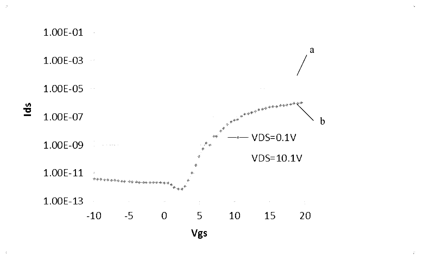
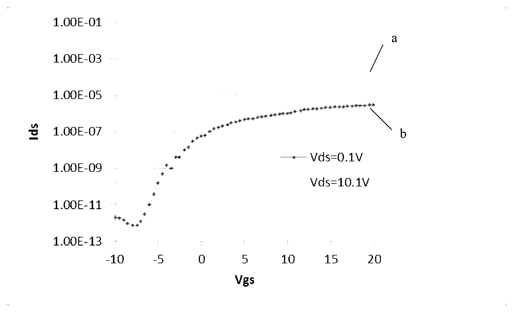
[0030] like image 3 As shown, it is a TFT threshold voltage compensation circuit in Embodiment 1 of the present invention, which includes: an input terminal, an output terminal connected to the source of the thin film transistor, the first resistor R1 to the Kth resistor RK connected in series in sequence, The Kth connectable link and at least one first connectable link, the K is a positive integer greater than 1, image 3 The Kth connectable link and the first connectable link are marked by adding a solid circle inside a hollow circle; where,

[0031] The Kth connectable link, which corresponds to the Kth resistor, is set between the input terminal and the output terminal, and is used for when the current threshold voltage of the thin film transistor is consistent with the set standard threshold voltage, Turning on the connection between the input terminal and the output terminal, and disconnecting the connection between the input terminal and the output terminal when the c...

Embodiment 2

[0050] Embodiment 2 of the present invention provides a shift register, and the shift register includes: an output terminal thin film transistor for controlling the output signal of the output terminal of the shift register;

[0051] Wherein, the source of the thin film transistor at the output end is connected to the thin film transistor threshold voltage compensation circuit described in Embodiment 1, and under the action of the compensation circuit, the gate and source of the thin film transistor at the output end The voltage difference is equal to its current threshold voltage.

[0052] Figure 5 The shown shift register composed of N-type TFTs is a shift register according to Embodiment 2 of the present invention. The thin film transistor at the output end of the shift register is M4, and its source is connected to the thin film transistor described in Embodiment 1. Transistor threshold voltage compensation circuit, therefore, if M4 is an amorphous silicon N-type TFT, if...

Embodiment 3

[0057] Embodiment 3 of the present invention provides a method for performing threshold voltage compensation on the compensation circuit described in Embodiment 1. The method includes:

[0058] When the current threshold voltage of the thin film transistor is consistent with the set standard threshold voltage, the connection between the input terminal and the output terminal is turned on; when the current threshold voltage of the thin film transistor is inconsistent with the set standard threshold voltage, the input terminal is disconnected. The connection between the terminal and the output terminal;

[0059] And when the current threshold voltage of the thin film transistor is inconsistent with the set standard threshold voltage, disconnect or conduct the connection between the output terminal and the kth resistor, where k is a positive value greater than or equal to 1 and less than or equal to K-1 integer.


PUM


Abstract

The invention discloses a TFT (thin film transistor) threshold voltage compensation method, a TFT (thin film transistor) threshold voltage compensation circuit, a shift register and a display device. The compensation circuit comprises an input end, an output end connected with a source electrode of a thin film transistor, a first resistor to a Kth resistor, which are sequentially connected with one another in series, a Kth connectable hinge and at least one connectable hinge, wherein the first resistor to the Kth resistor jointly divide the supply voltage input to the input end under the action of the switching on or off of the connectable hinges to control the voltage difference between a grid electrode and a source electrode of the thin film transistor to be equal to the current threshold voltage. In the scheme of the embodiment of the invention, a voltage division circuit with the connectable hinges is used for dividing the voltage input to the source electrode of the thin film transistor), so that when the voltage of the grid electrode of the thin film transistor is invariable, the voltage of the grid electrode and the source electrode of the thin film transistor is changed by changing the voltage of the source electrode; and therefore, the leakage current of the thin film transistor when the thin film transistor is turned off can be controlled, and the thin film transistor can be normally turned on and off.

Description

technical field [0001] The present invention relates to the field of display technology, in particular to a thin film transistor (Thin Film Transistor, TFT) threshold voltage compensation circuit and method, a shift register and a display device. Background technique [0002] Gate-driver on Array (GOA) technology can use TFT to realize the circuit function of the shift register, and integrate the shift register on the pixel array substrate. GOA and the pixel substrate can be completed under the same process technology, thus simplifying the production process of the entire display device. [0003] Although the GOA technology has the above advantages, its current problem is that the shift register integrated on the array substrate is highly dependent on the characteristics of the TFT, especially the current threshold voltage of the TFT has a huge impact on the stability of the shift register. . This is because the non-uniformity of the current threshold voltage or the deviat...

Claims


Application Information

Patent Timeline
IPC IPC(8): G11C19/28G09G3/20
CPCG11C19/28G09G3/3241G09G2300/043G09G2310/0286
Inventor 梁逸南马利飞皇甫鲁江
Owner BOE TECH GRP CO LTD
Why Eureka
Try Eureka