Display substrate, display device and manufacturing method of display substrate

A technology for display substrates and manufacturing methods, applied in optics, instruments, electrical components, etc., can solve problems such as product yield decline, picture display quality decline, color film surface unevenness, etc., to eliminate height differences and improve picture display quality , Improve the effect of flatness

Active Publication Date: 2013-08-07
BOE TECH GRP CO LTD
View PDF5 Cites 12 Cited by
  • Summary
  • Abstract
  • Description
  • Claims
  • Application Information

AI Technical Summary

Problems solved by technology

[0006] The purpose of the present invention is to provide a display substrate, a display device, and a method for manufacturing a display substrate, so as to solve the problem that the surface of the color filter is uneven, resulting in a decrease in the yield of the product and a decrease in the quality of the screen display.

Method used


Image

  • Display substrate, display device and manufacturing method of display substrate
  • Display substrate, display device and manufacturing method of display substrate
  • Display substrate, display device and manufacturing method of display substrate

Examples


Embodiment 1

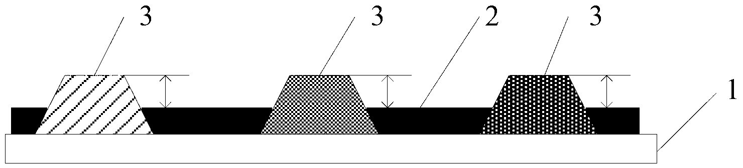
[0023] The display substrate provided by the embodiment of the present invention, such as figure 1 As shown, it includes a substrate substrate 1, a black matrix 2 formed on the substrate substrate 1, and a color filter 3 formed on the substrate substrate 1 with a height difference from the black matrix 2, and also includes: located on the black matrix 2, Or a flat layer located on the black matrix 2 and the color filter 3 , the flat layer is used to flatten the height difference between the black matrix 2 and the color filter 3 .

[0024] Further, in the embodiment of the present invention, the planarization layer used to planarize the height difference between the black matrix 2 and the color filter 3 can be preferably photoresist, which can be produced by simple photolithography technology, simplifying the production process.

[0025] When the photoresist is selected as the flat layer in the embodiment of the present invention, the schematic diagram of the substrate structur...

Embodiment 2

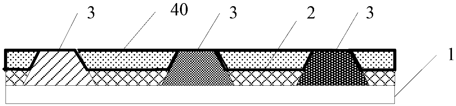
[0029] In the display substrate provided by Embodiment 2 of the present invention, a transparent photoresist is selected as the flat layer, and the transparent photoresist can be placed on the color film, such as image 3 Shown is a schematic diagram of the display substrate structure provided by the embodiment of the present invention, including a substrate substrate 1, a black matrix 2 formed on the substrate substrate 1, and a color filter 3 formed on the substrate substrate 1 with a height difference from the black matrix 2 , also includes: a transparent photoresist 41 located on the black matrix 2 and the color filter 3, wherein the upper surface of the transparent photoresist 41 is a horizontal plane, that is, the transparent photoresist 41 is at the position of the corresponding area of ​​the black matrix 2 Different layer heights than those in the corresponding regions of the color filter 3 eliminate the height difference between the black matrix 2 and the color filter ...

Embodiment 3

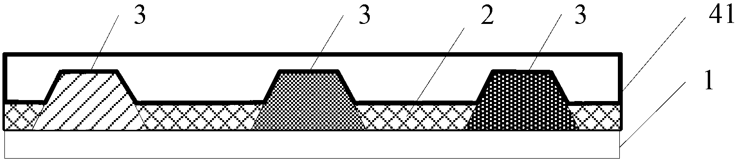
[0032] In the display substrate provided in Embodiment 3 of the present invention, the flat layer includes a transparent resin 42 and a photoresist 43, the transparent resin 42 covers the black matrix 2 and the color filter 3, and the photoresist 43 covers the transparent resin corresponding to the area of ​​the black matrix 2, And the upper surface of the photoresist 43 is located on the same horizontal plane as the upper surface of the transparent resin corresponding to the color filter area, such as Figure 4 shown.

[0033] It should be noted that the material of the transparent resin 42 in the embodiment of the present invention may be a transparent organic resin material, a transparent inorganic resin material or other materials that can achieve the purpose of the present invention.

[0034] The embodiment of the present invention provides a flat layer comprising transparent resin and photoresist. Due to the double-layer structure, the height difference between the black...


PUM


Abstract

The invention discloses a display substrate, a display device and a manufacturing method of the display substrate to solve the problems of yield decline and picture display quality decline of products due to the fact that the surface of a colored film is unsmooth. A flattening layer used for flattening the height difference between a black matrix and the colored film is formed on the black matrix or the colored film, or the flattening layer used for flattening the height difference between the black matrix and the colored film is formed on the black matrix, so that the height difference between the black matrix and the colored film can be well eliminated, and the surface smoothness of the colored film, the product yield and the picture display quality can be effectively improved.

Description

technical field [0001] The present invention relates to the field of display technology, in particular to a display substrate, a display device and a method for manufacturing the display substrate. Background technique [0002] With the reduction of the manufacturing cost and the improvement of the manufacturing process of the display panel, its application becomes more and more extensive. [0003] The display panel is generally composed of a display substrate, and the display substrate generally includes at least a substrate 1, a black matrix 2 formed on the substrate 1, and a color filter formed on the substrate 1 in the pixel area defined by the black matrix 2 3. The color filter 3 generally includes a red resin layer, a green resin layer and a blue resin layer, and the color filter 3 and the black matrix 2 are arranged at intervals, such as figure 1 shown. [0004] The manufacturing method of the display substrate in the current technology is to first form the pattern ...

Claims


Application Information

Patent Timeline
Patent Type & Authority Applications(China)
IPC IPC(8): G02F1/1335G02F1/1333
CPCG02F1/133514G02F2201/48G02F1/133512G02F1/133516G02B5/201G02F1/133357G02F1/133519H10K50/865H10K59/38
Inventor 张文林周伟峰
Owner BOE TECH GRP CO LTD
Why Eureka
Try Eureka