Thin film hybrid integrated circuit electroplating method

A hybrid integrated circuit and thin film technology, applied in the manufacturing of circuits, electrical components, semiconductor/solid-state devices, etc., can solve the problems of reduced production efficiency, high production cost, waste of precious metals, etc., and achieve high production efficiency, low production cost, circuit high precision effect

Inactive Publication Date: 2013-08-07
THE 41ST INST OF CHINA ELECTRONICS TECH GRP
View PDF4 Cites 12 Cited by
  • Summary
  • Abstract
  • Description
  • Claims
  • Application Information

AI Technical Summary

Problems solved by technology

[0003] At present, these three technologies have some deficiencies in the application process to varying degrees. For example, the first full-board electroplating, due to the thick electroplating film layer, has a large corrosion factor in wet etching, which makes the strip line size smaller. The precision becomes poor, and the waste of precious metals in this process is serious, and the production cost is high; for example, the second type requires gold wire bonding and gold wire removal processes, which inevitably produces a large number of metal scratches and burrs, increasing circuit loss and Standing wave coefficient, and the work of gold wire bonding and gold wire removal is labor-intensive and low-efficiency; while the third pattern electroplating technology is carried out with glue, and the photoresist will gradually integrate into the plating process during the electroplating process. In the electroplating solution, the electroplating current density that can be tolerated becomes smaller after the electroplating solution is polluted, and the production efficiency is reduced. In serious cases, the electroplating solution is scrapped

Method used


Image

  • Thin film hybrid integrated circuit electroplating method
  • Thin film hybrid integrated circuit electroplating method
  • Thin film hybrid integrated circuit electroplating method

Examples


Embodiment 1

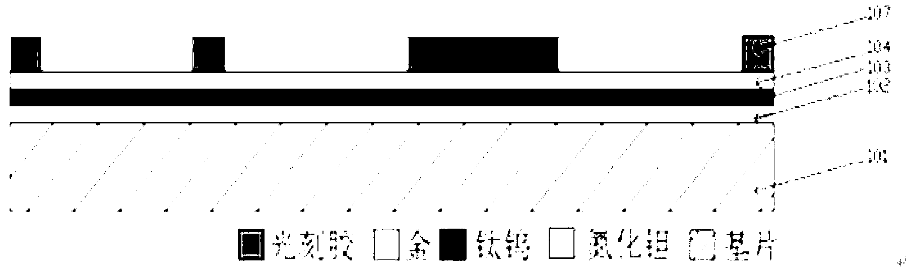
[0041] like Figure 1a to Figure 3 As shown, the present application provides a technical solution. The overall technical solution of the present invention is to utilize a magnetron vacuum sputtering machine to deposit TaN-TiWu-Au composite thin films sequentially on a microstrip substrate, and adjust the reaction gas flow ratio and time by controlling, Control the square resistance value of the film after sputtering to be lower than the design value of 5Ω∽15Ω, and the sputtering thickness of TiWu layer and Au layer is sputtered according to the design requirements; then use photoresist as a mask, and wet etching process Etch away the gold layer and titanium-tungsten layer and keep the tantalum nitride layer intact to realize the interconnection of the partial island circuit plating; then perform thermal oxidation treatment in a drying oven at 200°C--280°C 180min∽360min, so that a layer of tantalum oxide is produced on the surface of the tantalum nitride layer. After the above...

Embodiment 2

[0043] On the basis of the above embodiments, the production of a 50Ω / □ thin film hybrid integrated circuit is taken as an example to perform partial gold plating.

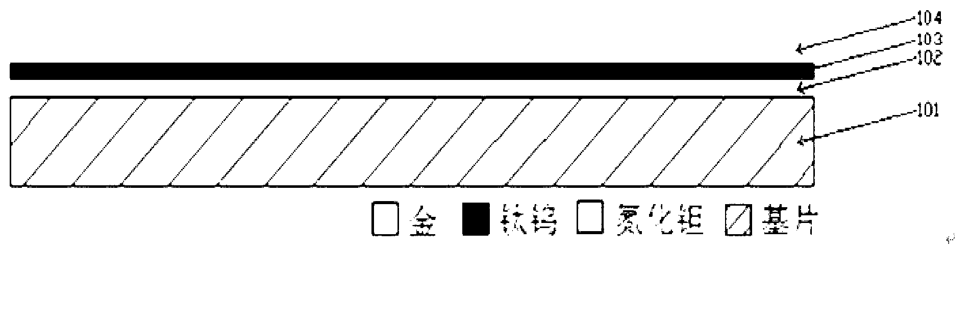
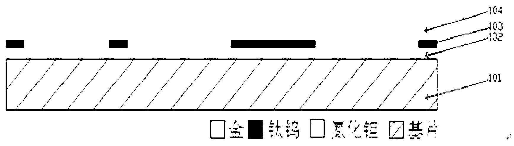
[0044] As shown in FIG. 1 , a circuit pattern is etched on the magnetron sputtering film with the tantalum nitride layer completely preserved.

[0045] like Figure 1a As shown, a tantalum nitride thin film resistor 102 is deposited on a substrate 101 by magnetron sputtering, using a high-purity tantalum target, the sputtering reaction gas is nitrogen and argon, and the gas flow partial pressure ratio is N2:Ar=1:35 , the thickness of the tantalum nitride film is 0.06 microns, and the square resistance of the film obtained by sputtering is 36∽45Ω / □, and then a titanium-tungsten target and a high-purity gold target are used, the sputtering reaction gas is argon, and the gas flow rate is 70sccm. A titanium-tungsten thin film 103 with a thickness of 0.05 micron and a gold thin film 104 with a thickness of 0.2 micron a...

Embodiment 3

[0055] On the basis of the above examples, if Figure 1a to Figure 3 Shown, a thin film hybrid integrated circuit electroplating method, wherein, comprises the following steps:

[0056] A: The tantalum nitride film resistor is deposited on the substrate by magnetron sputtering, using a high-purity tantalum target, and the sputtering reaction gas is nitrogen and argon;

[0057] B: Sputtering titanium-tungsten film and gold film on the tantalum nitride film in sequence, using titanium-tungsten target and high-purity gold target, and the sputtering reaction gas is argon;

[0058] C: Use photoresist as a mask, use a gold etching solution prepared with a mixed aqueous solution of iodine and potassium iodide to etch away unnecessary gold other than the design pattern, and use a titanium-tungsten etching solution to wet etch away the unnecessary gold outside the design pattern Titanium tungsten film;

[0059] D: After removing the photoresist with potassium hydroxide solution, rins...


PUM


Abstract

The invention provides a thin film hybrid integrated circuit electroplating method. The method includes: sequentially depositing a TaN-TiWu-Au composite thin film on a microstrip substrate by utilizing a magnetic-control vacuum sputtering machine, using photoresist as a mask, etching away a gold layer and a TiWu layer through the wet etching process and completely retaining a TaN layer for realizing interconnection when locally electroplating an island circuit; and performing thermal oxidation processing in a drying box at the temperature of 200-280 DEG C for 180-360min to generate a tantalum oxide layer on the surface of the TaN layer, by the above processing, local circuit connection and relative insulation on a non-electroplated surface under the electroplating state can be realized so as to realize selectively local electroplating. By the thin film hybrid integrated circuit electroplating method, photoresist consumption is small, production cost is low, and environment-friendly production development trend is met.

Description

technical field [0001] The invention relates to an electroplating technology, in particular to an electroplating method for a thin film hybrid integrated circuit. Background technique [0002] With the continuous advancement of microwave and millimeter wave technology, the manufacturing process of thin film hybrid integrated circuits has also greatly improved. Since the film thickness of vacuum sputtering or evaporation is less than 1 micron, in order to ensure that the circuit loss is as small as possible, it is necessary to The film thickness is increased to 3∽5 times of the skin depth, so it needs to be thickened by electroplating. At present, the material of thin film circuits is mostly gold, because it has stable performance, is not easy to oxidize, is not easy to be corroded by acid and alkali, and is conductive. Excellent performance and low circuit loss, but there are always isolated island circuits in the circuit. At present, there are three main electroplating tech...

Claims


Application Information

Patent Timeline
Patent Type & Authority Applications(China)
IPC IPC(8): H01L21/70
Inventor 樊明国
Owner THE 41ST INST OF CHINA ELECTRONICS TECH GRP
Why Eureka
Try Eureka