Preparation method of dye-sensitized metal sulfide semiconductor nanomaterial
A metal sulfide, dye sensitization technology, applied in chemical instruments and methods, zinc sulfide, cadmium sulfide, etc., can solve the problems of low quantum efficiency, uneven grain dispersion, easy to photocorrosion, etc., to achieve uniform dispersion, High photocatalytic degradation rate and adjustable grain size
- Summary
- Abstract
- Description
- Claims
- Application Information
AI Technical Summary
Problems solved by technology
Method used
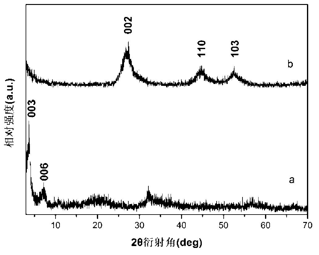
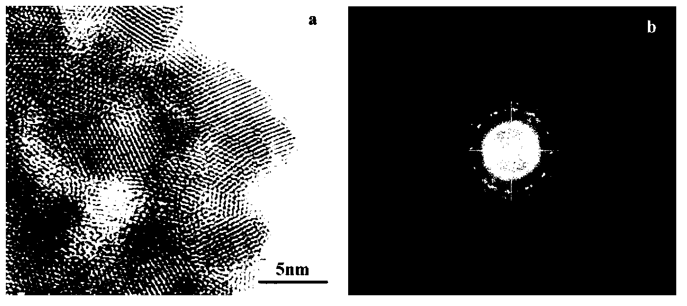
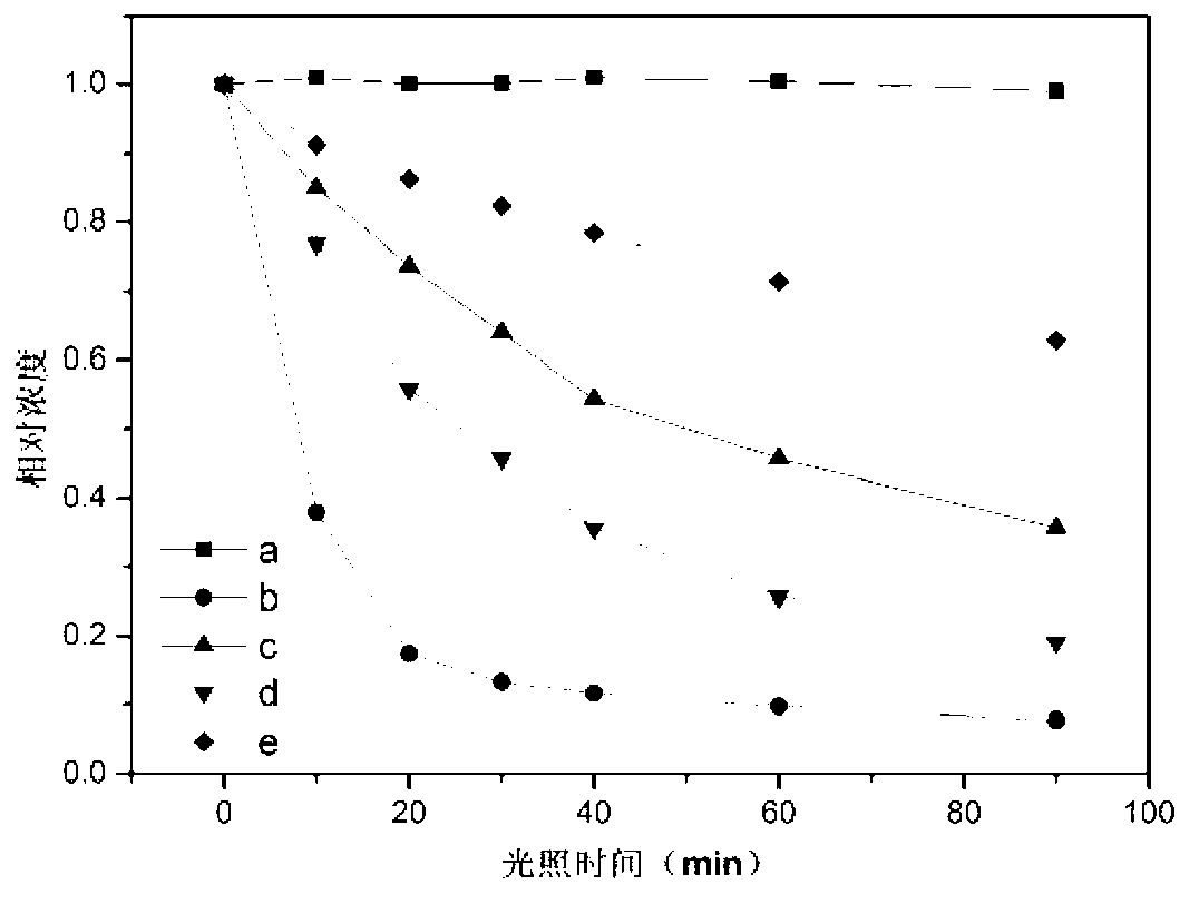
Image

Examples
Embodiment 1
[0022] Step A: Add 0.02 mol of Zn(NO 3 ) 2 ·6H 2 O, 0.01mol of Cd(NO 3 ) 2 ·4H 2 O and 0.01 mol of Al (NO 3 ) 3 ·9H 2 Dissolve O in 15 ml of de-CO 2 In water, add 0.02 mol of sodium dodecyl sulfate (C 12 H 25 NaO 4 S) Dissolve in 85ml of de-CO 2 In water, stir the two solutions to obtain a mixed salt solution; weigh 4g of NaOH and add it to 50ml to remove CO 2 Prepared in water to 2mol·L –1 NaOH solution;
[0023] Step B: 2mol L prepared in Step A –1 The NaOH solution was added dropwise to the mixed salt solution prepared in step A until the pH value of the system reached 8.0, crystallized at 25 °C for 8 hours, and CO was removed. 2 The obtained slurry was fully centrifuged and washed with water, and dried under vacuum conditions to obtain a sulfonate intercalated hydrotalcite precursor, denoted as Zn 2 Cd 1 Al-LDHs;
[0024] Step C: Place the hydrotalcite precursor prepared in Step B in a vulcanization reaction device, and mix it with H at 90°C. 2 S gas rea...
Embodiment 2
[0030] Step A: Add 0.02 mol of Zn(NO 3 ) 2 ·6H 2 O, 0.01mol of Cd(NO 3 ) 2 ·4H 2 O and 0.01 mol of Al (NO 3 ) 3 ·9H 2 Dissolve O in 15 ml of de-CO 2 In water, add 0.03 mol of sodium dodecyl sulfate (C 12 H 25 NaO 4 S) Dissolve in 85ml of de-CO 2 In water, stir the two solutions to obtain a mixed salt solution; weigh 4g of NaOH and add it to 50ml to remove CO 2 Prepared in water to 2mol·L –1 NaOH solution;
[0031] Step B: 2mol L prepared in Step A –1 The NaOH solution was added dropwise to the mixed salt solution prepared in step A, until the pH value of the system reached 8.0, crystallized at 25 °C for 14 hours, and CO was removed. 2 The obtained slurry is fully washed and centrifuged with water for many times, and dried under vacuum conditions to obtain Zn. 2 Cd 1 Al-LDHs;
[0032] Step C: The hydrotalcite precursor prepared in Step B is placed in a vulcanization reaction device, and is mixed with H at 80 °C. 2 S gas reaction for 60min, H 2 The flow rate ...
Embodiment 3
[0036] Step A: 0.01 mol of Zn(NO 3 ) 2 ·6H 2 O, 0.02mol of Cd(NO 3 ) 2 ·4H 2 O and 0.01 mol of Al (NO 3 ) 3 ·9H 2 Dissolve O in 15 ml of de-CO 2 In water, add 0.04 mol of sodium dodecyl sulfate (C 12 H 25 NaO 4 S) Dissolve in 85ml of de-CO 2 In water, stir the two solutions to obtain a mixed salt solution; weigh 4g of NaOH and add it to 50ml to remove CO 2 Prepared in water to 2mol·L –1 NaOH solution;
[0037] Step B: 2mol L prepared in Step A –1 The NaOH solution was added dropwise to the mixed salt solution prepared in step A until the pH value of the system reached 8.0, crystallized at 25 °C for 20 h, and CO was removed with 2 The obtained slurry is fully washed and centrifuged with water for many times, and dried under vacuum conditions to obtain Zn. 1 Cd 2 Al-LDHs;
[0038] Step C: Place the hydrotalcite precursor prepared in Step B in a vulcanization reaction device, and mix it with H at 90°C. 2 S gas reaction for 90min, H 2 The flow rate of S gas is ...
PUM
| Property | Measurement | Unit |
|---|---|---|
| size | aaaaa | aaaaa |
Abstract
Description
Claims
Application Information
 - R&D
- Intellectual Property
- Life Sciences
- Materials
- Tech Scout
- Unparalleled Data Quality
- Higher Quality Content
- 60% Fewer Hallucinations
Browse by: Latest US Patents, China's latest patents, Technical Efficacy Thesaurus, Application Domain, Technology Topic, Popular Technical Reports.
© 2025 PatSnap. All rights reserved.Legal|Privacy policy|Modern Slavery Act Transparency Statement|Sitemap|About US| Contact US: help@patsnap.com