LED backlight and liquid crystal display device
A technology of LED backlight source and liquid crystal display device, which is applied to static indicators, instruments, etc., can solve the problems of affecting the display of liquid crystal display device and the inability of LED backlight source to provide display light source.
- Summary
- Abstract
- Description
- Claims
- Application Information
AI Technical Summary
Problems solved by technology
Method used
Image
Examples
Embodiment 1
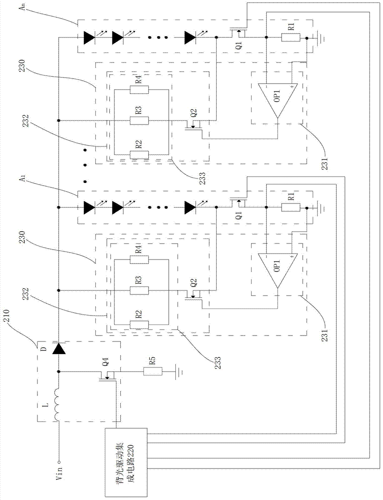
[0024] figure 2 A circuit diagram of an LED backlight source for a liquid crystal display device according to Embodiment 1 of the present invention is shown.
[0025] Such as figure 2 As shown, according to Embodiment 1 of the present invention, the LED backlight for the liquid crystal display device is set opposite to the liquid crystal display panel, and the LED backlight provides a display light source to the liquid crystal display panel, so that the liquid crystal display panel displays images, and the LED backlight The source includes a boost circuit 210, N LED strings A connected in parallel 1 ,...,A n , a backlight driving integrated circuit 220 and N control circuits 230, wherein, N is an integer greater than zero.
[0026] The boost circuit 210 is used to boost the input DC voltage Vin and output the boosted DC voltage.
[0027] N LED strings A 1 ,...,A n Used to provide a display light source to the liquid crystal display panel, each LED string includes a plu...
Embodiment 2
[0047] In Embodiment 2, in order to avoid unnecessary repetition, only the differences between Embodiment 2 and Embodiment 1 are described.
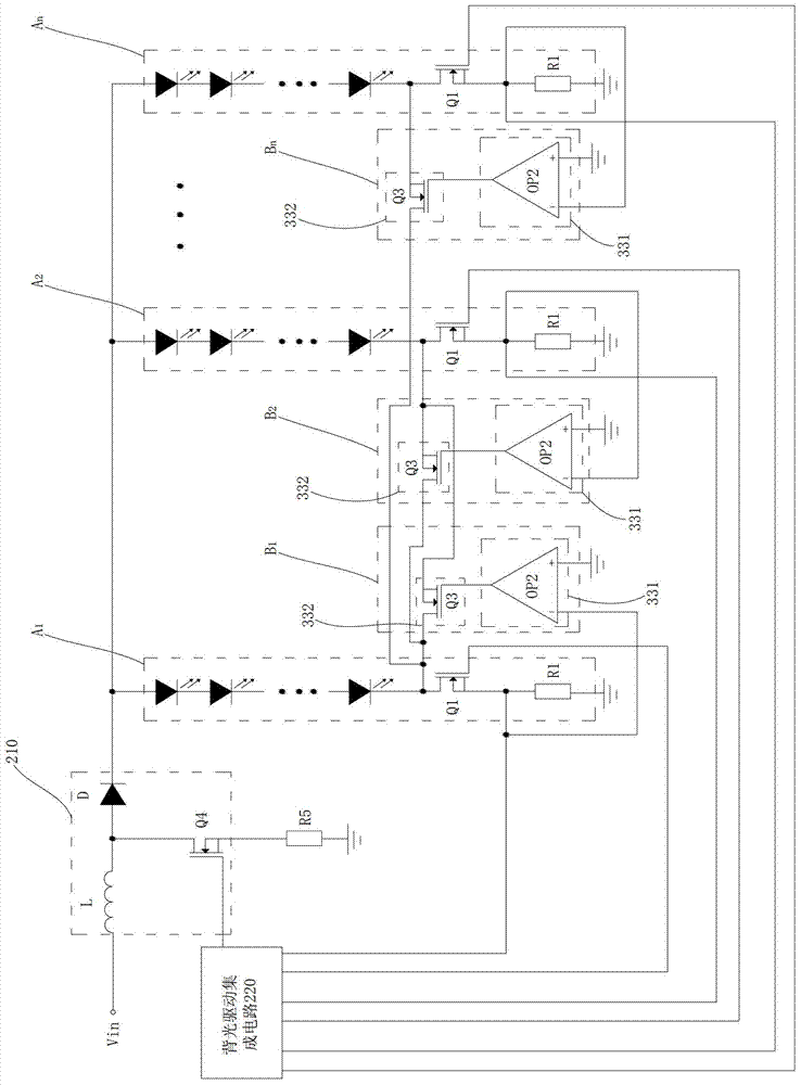
[0048] image 3 A circuit diagram of an LED backlight source for a liquid crystal display device according to Embodiment 2 of the present invention is shown.
[0049] Such as image 3 As shown, in each control circuit of the LED backlight according to Embodiment 2 of the present invention, the open circuit detection unit 331 includes an operational amplifier OP2, and the open circuit trigger protection unit 332 includes a MOS transistor Q3.
[0050] In each control circuit, the positive terminal of the operational amplifier OP2 is grounded, the output terminal of the operational amplifier OP2 is connected to the gate of the MOS transistor Q3, and the drain of the MOS transistor Q3 is connected to the drain of the MOS transistor Q1 in the first LED string.
[0051] where, in the first control circuit B 1 , the negative terminal of the ...
PUM
 Abstract
Description
Claims
Application Information


