Field emission display and fabrication method thereof

A display and field emission technology, which is applied in cold cathode manufacturing, electrode system manufacturing, electrode assembly manufacturing, etc., can solve problems such as inability to grow CNTs, difficult to synthesize CVD stable structures, etc., and achieve low price, simple manufacturing, and stable structure.

Inactive Publication Date: 2013-08-28
SN DISPLAY CO LTD
View PDF4 Cites 7 Cited by
  • Summary
  • Abstract
  • Description
  • Claims
  • Application Information

AI Technical Summary

Problems solved by technology

With the help of currently known CVD methods, it is difficult to synthesize CVD to have a stable structure at temperatures below 600 °C, so CNTs with a stable structure cannot be grown on low-priced glass substrates that are widely used in displays

Method used


Image

  • Field emission display and fabrication method thereof
  • Field emission display and fabrication method thereof
  • Field emission display and fabrication method thereof

Examples


Embodiment Construction

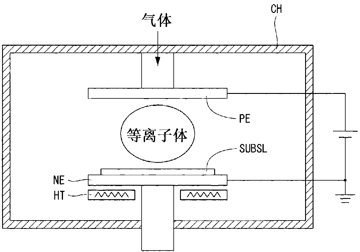
[0039] The field emission display (FED) of the present invention includes: an upper plate including an anode electrode and phosphor powder formed on an upper substrate; a lower plate facing the upper plate, and on the upper plate There is a vacuum space gap between the board and the lower board, the lower board includes a plurality of thin film patterns formed on a lower substrate; and a spacer is provided between the upper board and the lower board to Maintain the vacuum space gap.

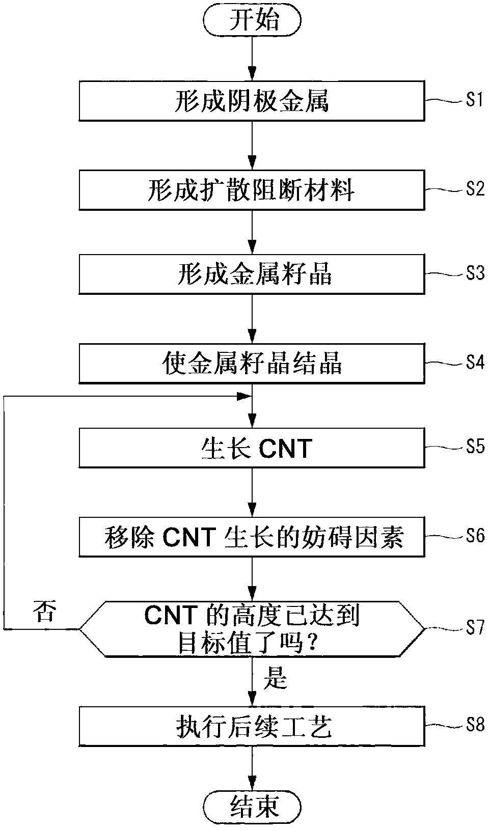
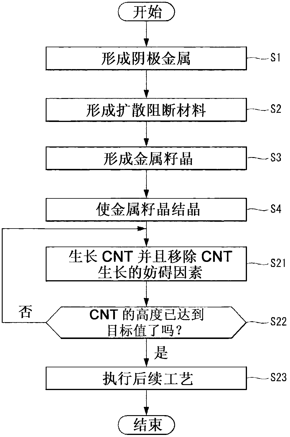
[0040] The lower plate may include: a cathode electrode including one or more metals selected from molybdenum (Mo), aluminum (Al), copper (Cu), chromium (Cr) and alloys thereof, and formed on the On the substrate; a diffusion barrier layer, the diffusion barrier layer includes titanium (Ti), tungsten (W), tantalum (Ta) and alloys of the three metals, silicon and any one or mixture of silicon compounds, and formed on the cathode electrode; a metal seed crystal formed on the diffusion blocking lay...


PUM

PropertyMeasurementUnit
thicknessaaaaaaaaaa
thicknessaaaaaaaaaa
thicknessaaaaaaaaaa

Abstract

A field emission display (FED) and a fabrication method thereof are disclosed. A lower plate of the FED includes: a cathode electrode formed on the substrate; a diffusion blocking layer formed on the cathode electrode; a seed metal layer formed on the diffusion blocking layer; carbon nano-tubes (CNTs) grown as single crystals from the grains of the seed metal layer; a gate insulating layer formed on the substrate on which the cathode electrode, the diffusion blocking layer, and the seed metal layer are formed, in order to cover the CNTs; and a gate electrode formed on the gate insulating layer.

Description

technical field [0001] The present application relates to a field emission display device including carbon nanotubes (CNTs) functioning as field emitters and a method of manufacturing the same. Background technique [0002] In a Field Emission Display (FED), an electric field is formed between a gate electrode and electron field emitters arranged at regular intervals on a cathode electrode to control electron emission from the field emitters, and when the emitted electrons When the phosphorus material collides, an image is displayed. [0003] Carbon nanotubes (CNTs) with very low work function and sharp structure have been discussed as field emitters for field emission displays. CNT synthesis methods include arc discharge, laser vaporization, pyrolysis, etc.; however, these methods include complex refining processes to obtain high purity after CNT synthesis, and have difficulties in structure control and vertical growth. Recently, chemical vapor deposition (CVD) capable of...

Claims


Application Information

Patent Timeline
Patent Type & Authority Applications(China)
IPC IPC(8): H01J1/30H01J9/02
CPCH01J1/304H01J3/021H01J9/025H01J9/148H01J31/127H01J2201/30469H01J2329/0455H01J2329/46Y10S977/952B82Y99/00H01J9/18
Inventor 李春來金学雄
Owner SN DISPLAY CO LTD
Why Eureka
Try Eureka