Embedded liquid crystal touch control panel
A touch panel and built-in technology, applied in instruments, computing, electrical digital data processing, etc., can solve the problems of cost increase, no space for color film substrate, and complicated manufacturing process, so as to improve integration and reduce cost Effect
- Summary
- Abstract
- Description
- Claims
- Application Information
AI Technical Summary
Problems solved by technology
Method used
Image

Examples
Embodiment 1
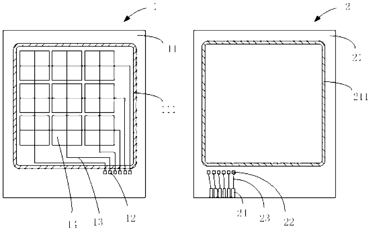
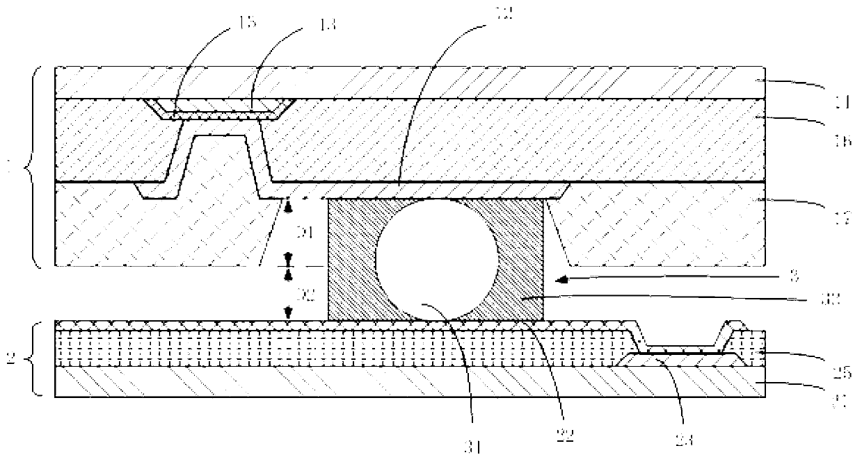
[0048] Please refer to figure 1 , figure 1 It is a schematic top view of the color filter substrate and the array substrate according to the first embodiment of the present invention. Among them, the color filter substrate 1 is located figure 1 On the left, array substrate 2 is located figure 1 Right. The color filter substrate 1 includes a transparent insulating substrate 11, and the transparent insulating substrate 11 may be a glass substrate or a resin substrate or the like. The transparent insulating substrate 11 (also called the color filter substrate 1 ) has a glue-sealed area 111 . The glue-sealed area 111 is an annular area formed around the periphery of the color filter substrate 1 . The glue-sealing area 111 is used for subsequent coating of frame glue, and the frame glue is used for glue-sealing the color filter substrate 1 and the array substrate 2 together to form a liquid crystal panel.
[0049] In this embodiment, the color filter substrate 1 includes a plu...
Embodiment 2
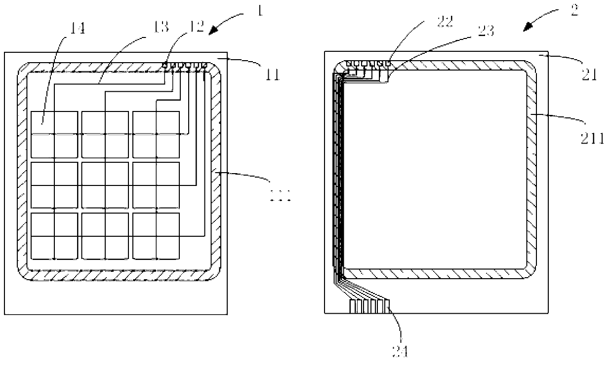
[0070] Please refer to image 3 , image 3 It is a schematic top view of the color filter substrate and the array substrate according to the second embodiment of the present invention. From image 3 It can be seen from the figure that in this embodiment, most of the structures of the color filter substrate 1 are the same as those of the first embodiment. However, the difference between the color filter substrate 1 of this embodiment and the first embodiment is that the first conductive pad 12 of this embodiment is disposed inside the glue-sealed area 111 located at the upper right corner of the color filter substrate 1 . Similarly, for image 3 The difference between the array substrate 2 in the first embodiment and the array substrate in the first embodiment is that the position of the second conductive pad 22 is changed. In this embodiment, the second conductive pad 22 also falls inside the glue sealing area 211 of the array substrate 2 . Moreover, since the position of...
Embodiment 3
[0075] Please refer to Figure 5 , Figure 5 It is a schematic top view of the color filter substrate and the array substrate according to the third embodiment of the present invention. From Figure 5 It can be seen from the figure that in this embodiment, most of the structure of the color filter substrate 1 is the same as that in the second embodiment, the difference is that in this embodiment the first conductive pad 12 is located in a region other than the glue-sealed region 111 . Specifically, the first conductive pad 12 is located at the upper right corner of the color filter substrate 1 . Likewise, in this embodiment, the second conductive pad 22 on the array substrate 2 is correspondingly located at the upper left corner of the array substrate 2 . In this embodiment, the second signal line 23 on the array substrate 2 is correspondingly arranged in the area other than the glue sealing area 211 , and the area where the second conductive pad 22 is located is the common...
PUM
| Property | Measurement | Unit |
|---|---|---|
| Diameter | aaaaa | aaaaa |
Abstract
Description
Claims
Application Information
 - Generate Ideas
- Intellectual Property
- Life Sciences
- Materials
- Tech Scout
- Unparalleled Data Quality
- Higher Quality Content
- 60% Fewer Hallucinations
Browse by: Latest US Patents, China's latest patents, Technical Efficacy Thesaurus, Application Domain, Technology Topic, Popular Technical Reports.
© 2025 PatSnap. All rights reserved.Legal|Privacy policy|Modern Slavery Act Transparency Statement|Sitemap|About US| Contact US: help@patsnap.com