Providing device and method of LED wafers

A wafer and positioning device technology, applied in electrical components, semiconductor/solid-state device manufacturing, circuits, etc., can solve the problems of low precision, high labor consumption, low productivity, etc., to reduce manufacturing costs, reduce the ratio of inferior quality, The effect of reducing engineering time

Inactive Publication Date: 2013-09-11
LG CNS +1
View PDF6 Cites 0 Cited by
  • Summary
  • Abstract
  • Description
  • Claims
  • Application Information

AI Technical Summary

Problems solved by technology

[0003] However, similar to the prior art, when the operator manually performs the operation, it takes too long, the productivity is low, the manpower consumption is large, and the precision is low.
[0004] In order to solve the above problems, although a series of automatic LED wafer supply devices are used in the prior art, there is still the problem of imperfect operability

Method used


Image

  • Providing device and method of LED wafers
  • Providing device and method of LED wafers
  • Providing device and method of LED wafers

Examples


Embodiment Construction

[0033] The technical configuration of the LED wafer supply device will be described in detail below with reference to the drawings.

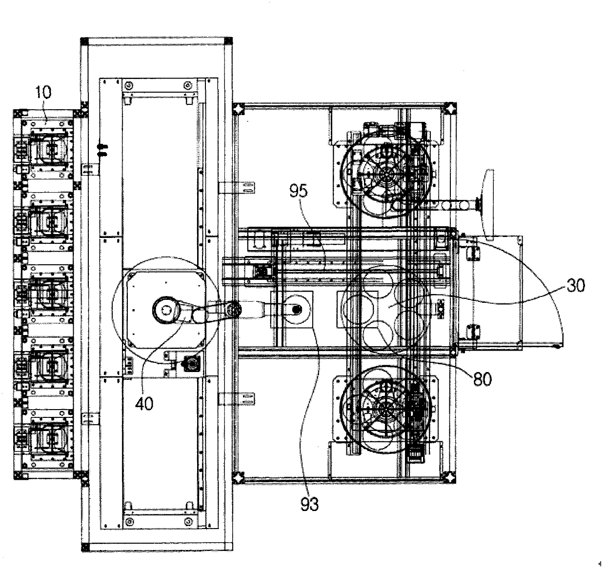
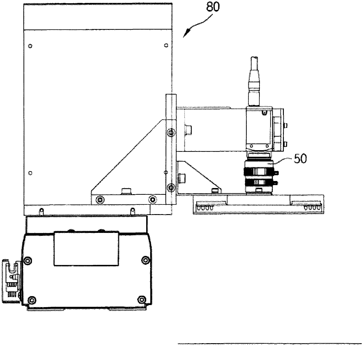
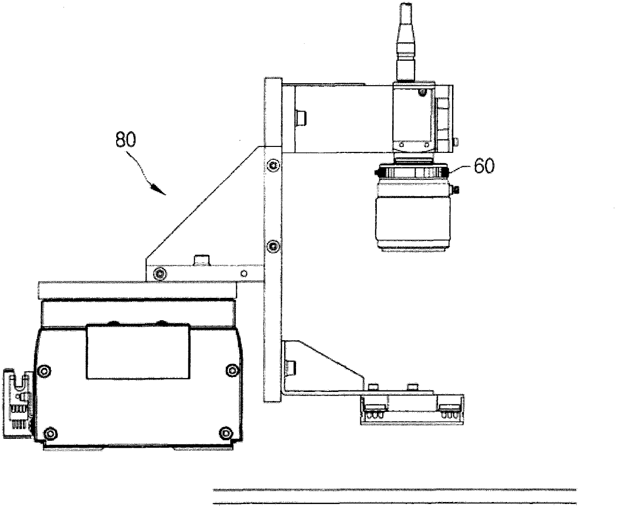
[0034] Such as Figure 1 to Figure 6 As shown, an LED wafer providing device according to an embodiment of the present invention includes a deck 10 , a carrier 30 , an arrangement unit 93 , a transfer robot 40 , a positioning device 20 , a camera unit 80 , and an LED wafer loading robot 95 . The cassette 10 is installed with a plurality of LED wafers 99 for loading; the carrier 30 is equipped with a plurality of containers 31 for arranging the LED wafers 99; the carrier 30 is formed in a disc shape, and the containers 31 are equipped radially. There are a plurality of them, and they are spaced apart at regular intervals in the circumferential direction based on the center of the disc-shaped carrier 30 .

[0035] The alignment unit 93 aligns the LED wafers 99 to be placed on the carrier 30 . In this case, the alignment of the LED wafer 99 is to...


PUM


Abstract

The invention provides a providing device and method of LED wafers. The providing device and method of the LED wafers can obtain the position information of a container of a carrier where the LED wafers are arranged to carry out accurate and fast transfer operation of the LED wafers. The providing device of the LED wafers comprises a clamping seat, the carrier, an arrangement unit, a transferring robot arm, a locating device, a camera shooting unit and an LED wafer loading robot arm. Multiple LED wafers are loaded on the clamping seat, the carrier is provided with multiple containers for containing the LED wafers, the arrangement unit arranges the LED wafers to be contained in the carrier, the transferring robot arm transfers the LED wafers from the clamping seat to the arrangement unit, the locating device adsorbs the LED wafers transferred to the arrangement unit and relieves the absorption, the camera shooting unit enables the locating device to be fixed to obtain the position information of the containers, and the LED wafer loading robot arm transfers the locating device and the camera shooting unit from the arrangement unit to the carrier. Therefore, the providing device and method of the LED wafers can load the LED wafers in the carrier fast and accurately, a whole engineering time is reduced, and an inferior ratio is obviously reduced.

Description

technical field [0001] The present invention relates to an LED wafer supply device and method, and more particularly, to a LED wafer supply device and method for transferring an LED wafer for vapor phase deposition (MOCVD) equipment loaded in a cassette to a carrier for supply. technical background [0002] Generally, hexagonal crystal wafers are used to manufacture light-emitting diodes (LEDs), and such LED wafers are provided in a state of being loaded on a carrier (Carrier) in a state where they are used for deposition, etc. In the engineering chamber (chamber). [0003] However, similarly to the prior art, when the operator manually performs the operation, it takes too long, the productivity is low, the manpower consumption is large, and the precision is low. [0004] In order to solve the above problems, although a series of automatic LED wafer supply devices are used in the prior art, there is still the problem of imperfect operability. Accordingly, there is a need f...

Claims


Application Information

Patent Timeline
IPC IPC(8): H01L21/67H01L33/00
Inventor 柳仁桓李学杓杨日灿崔圣奎李炳承
Owner LG CNS
Why Eureka
Try Eureka