TSV or TGV pinboard, 3D packaging and manufacture method thereof

An adapter board, packaging structure technology, applied in the direction of semiconductor/solid-state device manufacturing, semiconductor/solid-state device components, semiconductor devices, etc., can solve the problem of large vertical size, unfavorable package miniaturization, sensitive chip and interference chip vertical interconnection spacing Remote and other problems, to achieve a convenient method, the effect of suppressing noise

Active Publication Date: 2013-09-11
NAT CENT FOR ADVANCED PACKAGING
View PDF6 Cites 23 Cited by
  • Summary
  • Abstract
  • Description
  • Claims
  • Application Information

AI Technical Summary

Problems solved by technology

In the POP package, the vertical interconnection distance between the sensitive chip and the interfering chip is far away, and the near-field couplin

Method used


Image

  • TSV or TGV pinboard, 3D packaging and manufacture method thereof
  • TSV or TGV pinboard, 3D packaging and manufacture method thereof
  • TSV or TGV pinboard, 3D packaging and manufacture method thereof

Examples


Embodiment 1

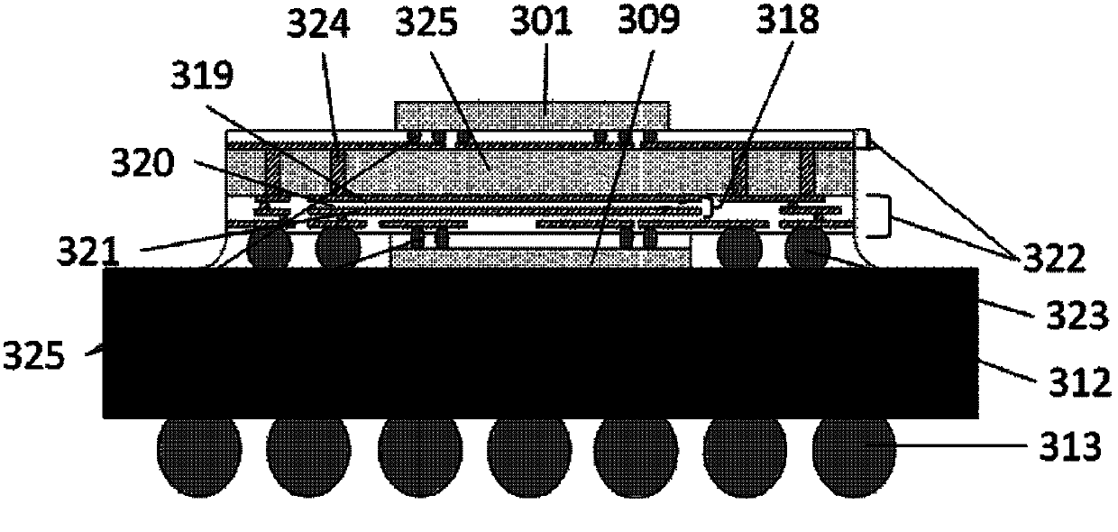
[0027] Such as figure 1In the shown 3D package structure, the redistribution layer 322 in the TSV interposer or the TGV interposer and the TSV or TGV 324 are used for signal interconnection in the interposer. The bare chips 301 , 309 are bonded on the TSV interposer or the TGV interposer by using micro-bumps 325 . The shielding structure 318 with EBG and the redistribution layer 322 are fabricated in the TSV and TGV interposers at the same time, and the same fabrication process and materials are used. The shielding structure includes a first-layer metal plane 319 , an insulating layer (or barrier layer) 320 and a second-layer metal plane 321 etched with a periodic EBG structure. The unit shape, number and even structural deformation of the periodic EBG structure are determined according to the noise frequency band to be suppressed. The insulating layer (or barrier layer) 320 adopts SiO 2 or Si 3 Ni 4 and other insulating materials. Solder balls 323 are used for electrica...

Embodiment 2

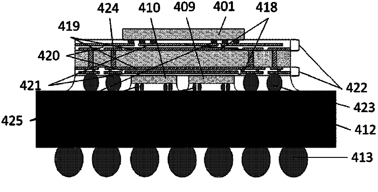
[0041] Such as figure 2 In the shown 3D package structure, the redistribution layer 422 in the TSV interposer or the TGV interposer and the TSV or TGV 424 are used for signal interconnection in the interposer. The bare chips 401 , 409 and 410 are bonded on the TSV and TGV adapter boards by using micro-bumps 425 . The shielding structure 418 with EBG and the redistribution layer 422 are fabricated in the TSV and TGV interposers at the same time, and the same fabrication process and materials are used. The shielding structure includes a first-layer metal plane 419, an insulating layer (or barrier layer) 420, and a second-layer metal plane 421 etched with a periodic EBG structure. The unit shape, number and even structural deformation of the periodic structure are determined according to the noise frequency band that needs to be suppressed. The insulating layer (or barrier layer) 420 adopts SiO 2 or Si 3 Ni 4 and other insulating materials. Solder balls 423 are used for el...


PUM


Abstract

The invention provides a TSV or TGV pinboard, 3D packaging and a manufacture method of the TSV or TGV pinboard and a manufacture method of the 3D packaging. A TSV or TGV pinboard with an EBG shielding structure comprises a TSV or TGV pinboard body and the EBG shielding structure. The EBG shielding structure is manufactured in the TSV or TGV pinboard, or manufactured on two sides of the TSV or TGV pinboard. The EBG shielding structure comprises an insulating layer and at least two metal planes, wherein, periodic EBG structures are etched in at least one metal plane, and the insulating layer is arranged between the metal planes. The invention further provides a manufacture method of the TSV or TGV pinboard and a manufacture method of the 3D packaging. The TSV or TGV pinboard, the 3D packaging and the manufacture method of the TSV or TGV pinboard and the manufacture method of the 3D packaging can effectively reduce the near field coupling problem among chips in perpendicular 3D interconnection packaging.

Description

technical field [0001] The invention relates to the technical field of microelectronic packaging, in particular to a TSV or TGV adapter plate with an electromagnetic band gap (Electromagnetic Band Gap, EBG) shielding structure, a 3D packaging structure and a preparation method thereof. Background technique [0002] With the rise of communication electronics, people's demand for miniaturized and high-sensitivity modules or systems is getting higher and higher, and the requirements for signal quality are becoming more and more stringent. High-density integration technologies, such as System-in-Package (SiP) technologies, have developed rapidly, but miniaturized integrated packaging of mixed-signal multi-chip systems has become one of the technical difficulties in this field. [0003] The frequency of digital signals continues to rise, and the rising / falling edges become more and more jittery. The high-frequency components of digital signals have an increasing impact on sensiti...

Claims


Application Information

Patent Timeline
IPC IPC(8): H01L23/552H05K9/00H01L21/768
CPCH01L2924/15311H01L2224/16225H01L2224/73204H01L2224/73253H01L2924/3025
Inventor 李君万里兮郭学平
Owner NAT CENT FOR ADVANCED PACKAGING
Why Eureka
Try Eureka