Shielding structure with EBG, 3D packaging structure and preparing method of shielding structure with EBG and 3D packaging structure

A shielding structure, 3D technology, applied in the direction of semiconductor/solid-state device components, semiconductor devices, electrical components, etc., can solve the problems of large vertical size, unfavorable package miniaturization, and long vertical interconnection distance between sensitive chips and interfering chips, etc., to achieve Convenient method, effect of suppressing noise

Active Publication Date: 2013-09-11
NAT CENT FOR ADVANCED PACKAGING
View PDF6 Cites 15 Cited by
  • Summary
  • Abstract
  • Description
  • Claims
  • Application Information

AI Technical Summary

Problems solved by technology

In the POP package, the vertical interconnection distance between the sensitive chip and the interfering chip is far away, and the near-field coupling problem is not too serious, but the vertical size of this package is relatively large, which is not conducive to the miniaturization of the package.

Method used


Image

  • Shielding structure with EBG, 3D packaging structure and preparing method of shielding structure with EBG and 3D packaging structure
  • Shielding structure with EBG, 3D packaging structure and preparing method of shielding structure with EBG and 3D packaging structure
  • Shielding structure with EBG, 3D packaging structure and preparing method of shielding structure with EBG and 3D packaging structure

Examples


Embodiment 1

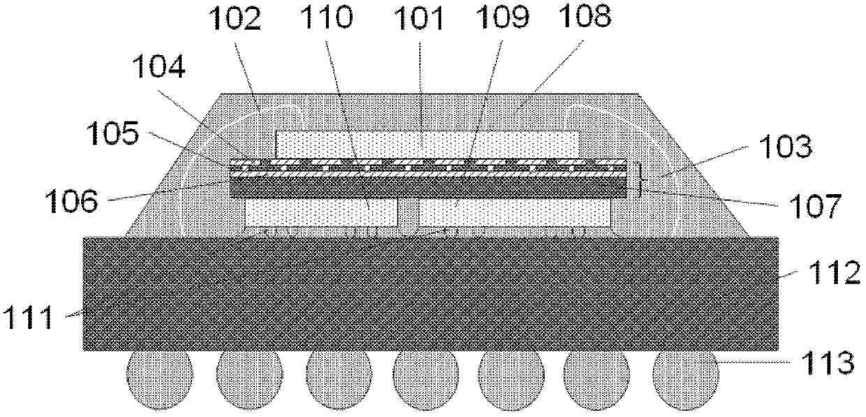
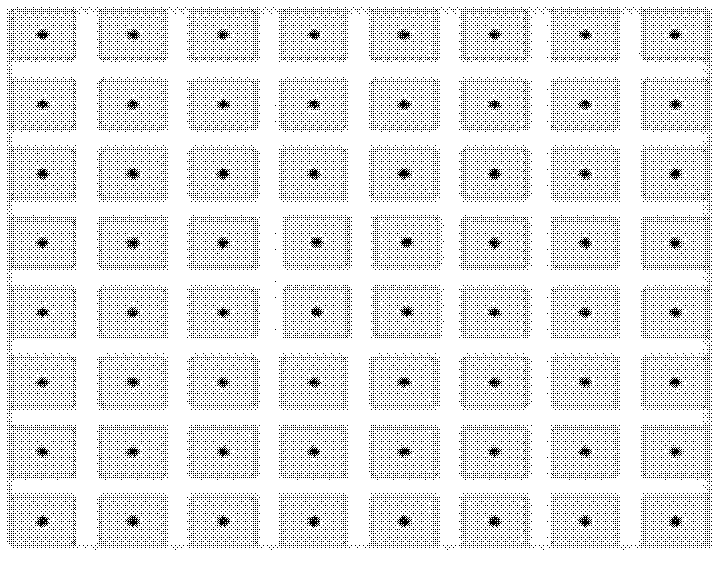
[0026] Such as figure 1 In the shown 3D packaging structure, the bare chips 109 and 110 are bonded on the interconnection substrate 112 by flip-chip bonding, and filled with underfill glue to protect the flip-chip bumps 111 . The individual shielding device 103 with the EBG structure is fixed on the bare chips 109 and 110 with an adhesive. The shielding device 103 includes a support plate 107, a first metal plane 106 etched with a periodic EBG structure, an insulating layer 105, and a second metal plane 104, wherein the unit shape, number and even structural deformation of the periodic EBG structure suppress noise as required Frequency band decision. The support plate can be a variety of substrates such as silicon-based or glass-based, organic substrates, and even ceramic substrates. The insulating material of the corresponding insulating layer 105 may be SiO 2 、Si 3 Ni 4 , organic substrate materials or ceramic materials and other materials. The bare chip 101 is fixed o...

Embodiment 2

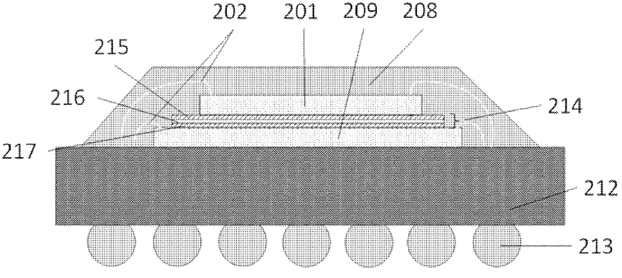
[0037] Such as figure 2 In the shown 3D packaging structure, the bare chip 209 is bonded on the interconnection substrate 212 by wire bonding. A separate shielding device 214 with an EBG structure is fixed on the bare chip 209 with an adhesive, and the shielding device 214 is prepared using a flexible substrate, including a first metal plane 217, an insulating layer 216, and a second metal layer etched with a periodic structure. Plane 215. Among them, the unit shape, quantity and even structural deformation of the periodic structure are determined according to the noise frequency band to be suppressed. The bare chip 201 is fixed on the shielding device 214 with an adhesive, and bonded to the interconnection substrate 212 by wire bonding. The bonding wire 202 is made of various materials such as gold wire, copper wire or aluminum wire. Potting compound 208 such as plastic encapsulant is filled between the 3D stacked bare chips 201 and 209 and the shielding device 214 to fix ...


PUM


Abstract

The invention provides a shielding structure with an EBG, a 3D packaging structure and a preparing method of the shielding structure with the EBG and the 3D packaging structure. The shielding structure with the EBG comprises an insulating layer and at least two metal planes. A periodical EBG structure is etched on at least one metal plane. The insulating layer is arranged between the two metal planes. The preparing method of the shielding structure with the EBG comprises the steps that at least one layer of metal plane is prepared, the middle insulating layer is prepared, and at least one layer of metal plane with the periodical EBG structure is prepared. The 3D packaging structure comprises the shielding structure with the EBG, an unpacked chip and an interconnected substrate. The unpacked chip is bonded to the interconnected substrate and connected with the shielding structure. The invention further provides the preparing method of the 3D packaging structure. The problem of near-field coupling between chips in perpendicular 3D interconnected packaging can be effectively solved.

Description

technical field [0001] The invention relates to the technical field of microelectronic packaging, in particular to a shielding structure with EBG (Electromagnetic Band Gap, EBG), a 3D packaging structure and a preparation method thereof. Background technique [0002] With the rise of communication electronics, people's demand for miniaturized and high-sensitivity modules or systems is getting higher and higher, and the requirements for signal quality are becoming more and more stringent. High-density integration technologies, such as System-in-Package (SiP) technologies, have developed rapidly, but miniaturized integrated packaging of mixed-signal multi-chip systems has become one of the technical difficulties in this field. [0003] The frequency of digital signals continues to rise, and the rising / falling edges become more and more jittery. The high-frequency components of digital signals have an increasing impact on sensitive circuits such as analog or RF chips. The sens...

Claims


Application Information

Patent Timeline
IPC IPC(8): H01L23/552
CPCH01L2924/15311H01L2224/16225H01L2224/32145H01L2224/32225H01L2224/48091H01L2224/48227H01L2224/73204H01L2224/73253H01L2924/3025H01L2924/00014H01L2924/00
Inventor 李君万里兮郭学平
Owner NAT CENT FOR ADVANCED PACKAGING
Why Eureka
Try Eureka