A high-power semiconductor laser transition heat sink and its preparation method
A technology of lasers and semiconductors, applied in semiconductor lasers, structural details of semiconductor lasers, lasers, etc., can solve problems such as laser damage, metal connection, bar damage, etc., to achieve smooth upper and lower surfaces, accurate size and accuracy Effect
- Summary
- Abstract
- Description
- Claims
- Application Information
AI Technical Summary
Problems solved by technology
Method used
Image
Examples
Embodiment 1
[0042] Embodiment 1. A method for manufacturing a high-power laser single-die transitional heat sink.
[0043] (1) Cut the SiC crystal with a single-wire swing cutting machine to obtain a SiC wafer with a flat upper and lower surface, a thickness of 400 μm, and a diameter of 2.5 inches. Such as figure 1 shown.
[0044] (2) Clean the SiC wafer obtained in step (1), soak the SiC wafer in sulfuric acid with a concentration of 90 wt% for half an hour, rinse the sulfuric acid on the surface with deionized water and blow dry with nitrogen.
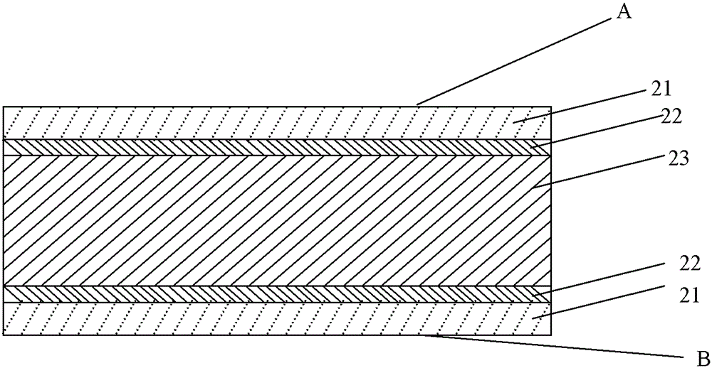
[0045] (3) The cleaned SiC wafer 23 is vapor-deposited metal titanium on the upper and lower surfaces respectively as a metal transition layer 22 with a thickness of 50 μm by vapor deposition; is 300μm; the metallized SiC wafer is obtained, and the cross-sectional view is as follows figure 2 As shown, the upper and lower surfaces of the wafer are A-side and B-side respectively.
[0046] (4) Making insulating grooves 24 on the surface A of t...
Embodiment 2
[0049] Embodiment 2. A method for preparing a high-power laser dual-die transitional heat sink.
[0050] As described in Embodiment 1, step (5) divides the finished product monolithic wafer obtained in step (4) into a single transitional heat sink for double-die encapsulation, Figure 5 Shown is a dual die transition heat sink that was laser scribed to image 3 The overall wafer shown is scribed and divided into Figure 5 The shape shown is cut with a straight line perpendicular to the insulation groove, a straight line parallel to the insulation groove, and a straight line where the insulation groove is located. Two insulation slots are reserved between the wires, which are used to wire the soldered die to the left side of the insulation slot, which is convenient for die stick testing and improves the subsequent packaging pass rate.
Embodiment 3
[0051] Embodiment 3, a preparation method of a high-power laser multi-die transitional heat sink
[0052] Steps (1), (2) are as in Example 1. The difference is:
[0053] (3) The cleaned SiC wafer 23 is vapor-deposited metal titanium on the upper and lower surfaces respectively as a metal transition layer 22 by vapor deposition, with a thickness of 45 μm; It is 200μm; the metallized SiC wafer is obtained, and the cross-sectional view is as follows figure 2 As shown, the upper and lower surfaces of the wafer are A-side and B-side respectively.
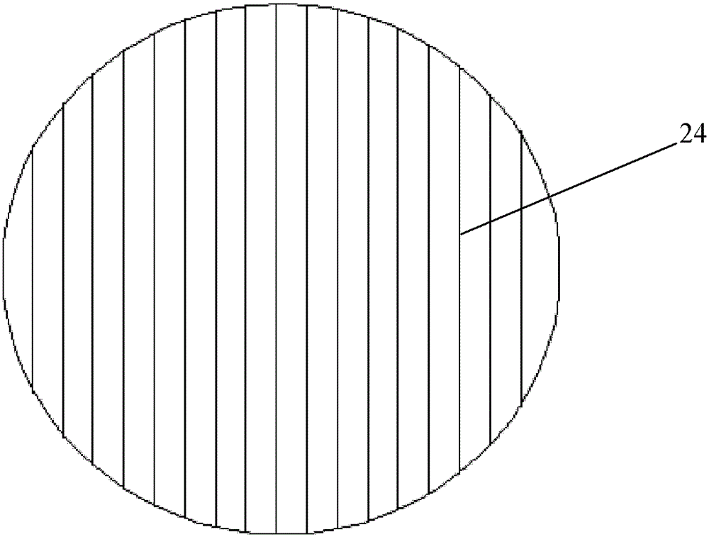
[0054] (4) Making insulating grooves 24 on the surface A of the metallized SiC wafer obtained in step (3) by ion etching, the width of the insulating grooves is 0.8 mm, and the interval of the insulating grooves is 3 mm. Such as image 3 shown. The depth of the insulating trench exposes the SiC wafer.
[0055] The method of ion etching is to use plasma to etch thin films. The plasma is accelerated by an electric field so that it h...
PUM
| Property | Measurement | Unit |
|---|---|---|
| thickness | aaaaa | aaaaa |
| thickness | aaaaa | aaaaa |
| thickness | aaaaa | aaaaa |
Abstract
Description
Claims
Application Information


