Method for laminating multilayer printed circuit board

A core board and outer layer technology, applied in the direction of multi-layer circuit manufacturing, etc., can solve problems such as unevenness of the PCB surface, and achieve the effect of overcoming the unevenness of the board surface and improving the production quality.

Inactive Publication Date: 2013-10-23
PEKING UNIV FOUNDER GRP CO LTD +1
View PDF7 Cites 5 Cited by
  • Summary
  • Abstract
  • Description
  • Claims
  • Application Information

AI Technical Summary

Problems solved by technology

[0006] The present invention aims to provide a lamination method of multi-layer PCB to solve the problem of uneven surface of PCB
[0008] The lamination method of the multilayer PCB in the embodiment of the present invention overcomes the problem of uneven PCB surface and improves the manufacturing quality of the PCB because the prefabricated core board is used to make the outer layer of the multilayer PCB.

Method used


Image

  • Method for laminating multilayer printed circuit board
  • Method for laminating multilayer printed circuit board

Examples


Embodiment Construction

[0012] The present invention will be described in detail below with reference to the accompanying drawings and in combination with embodiments.

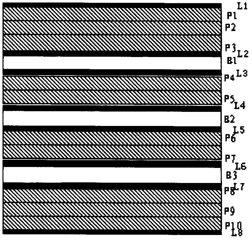
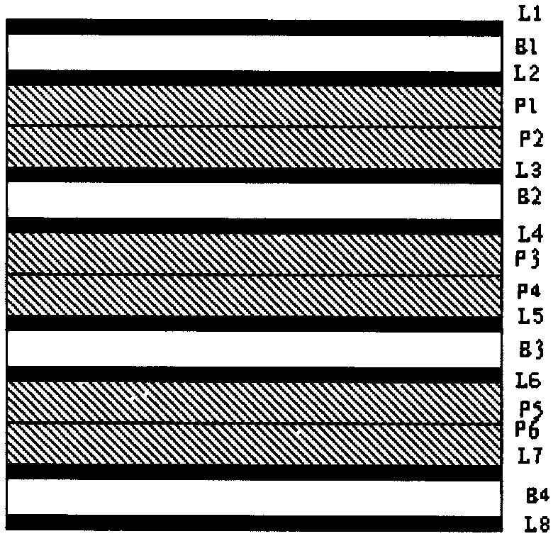
[0013] Embodiments of the present invention provide a method for laminating multilayer PCBs. A prefabricated core board is used to make the outer layer of a multilayer PCB, wherein the core boards are composed of two conductive layers and a curing sheet, and the curing sheet is located between two Between the two conductive layers, the two conductive layers respectively constitute the outer layer and the sub-outer layer of the multilayer PCB.

[0014] in such as figure 1 In the related technology shown, the outermost conductive layers L1 and L8 use separate copper foils for temporary thermocompression bonding, and P1, P2 and P3, and P8, P9 and P10 are in a flowing state during the lamination process, so Both the conductive layer L1 and the conductive layer L8 are affected by other internal conductive layers L2, L3, L4, L5, L6 and L7...


PUM


Abstract

The invention provides a method for laminating a multilayer printed circuit board. An outer layer of the multilayer printed circuit board (PCB) is manufactured by adopting a prefabricated core board, wherein the core board is formed by two conductive layers and a solidification piece, the solidification piece is located between the two conductive layers, and the two conductive layer form an outer layer and a secondary outer layer of the multilayer PCB respectively. The method provided by the invention overcomes a problem of unevenness of the PCB surface, and improves the manufacturing quality of the PCB.

Description

technical field [0001] The invention relates to the field of printed circuit boards (PCBs), in particular to a lamination method for multilayer PCBs. Background technique [0002] A multilayer printed circuit board is a printed circuit board formed by alternately laminating and bonding more than three layers of conductive pattern layers (usually copper foil) and insulating material (ie substrate) layers, and meets the design requirements. Conductive pattern interconnection between layers. The lamination technology of the so-called multilayer printed circuit board refers to a sheet material made by using a cured sheet (impregnated with epoxy resin by glass cloth and then baked to remove the solvent. The resin is in the B stage, under the action of temperature and pressure It has fluidity and can quickly solidify and complete bonding.) The technology of bonding conductive patterns under high temperature and high pressure. [0003] figure 1 A schematic diagram of a laminatio...

Claims


Application Information

Patent Timeline
Patent Type & Authority Applications(China)
IPC IPC(8): H05K3/46
Inventor 刘茂林
Owner PEKING UNIV FOUNDER GRP CO LTD
Why Eureka
Try Eureka