Test structure of transistor alternating current hot carrier injection characteristics

A technology for testing structures and hot carriers, which is applied in the testing of single semiconductor devices, electric solid-state devices, semiconductor devices, etc., can solve the problem that the evaluation effect cannot be achieved, it is difficult to control the synchronization of two signals, and it cannot truly simulate the working state of CMOS. and other problems to achieve the effect of saving evaluation time

Active Publication Date: 2013-10-30
SHANGHAI HUAHONG GRACE SEMICON MFG CORP
View PDF4 Cites 7 Cited by
  • Summary
  • Abstract
  • Description
  • Claims
  • Application Information

AI Technical Summary

Problems solved by technology

When this independent structure is loaded with AC HCI stress, it can only load an AC signal on one end (gate or drain), and the other end is a DC signal, which cannot truly simulate the working state of the CMOS in the circuit and cannot achieve the best evaluation. Effect
If AC signals are applied to the two ends (gate and drain) of the MOS device through two different devices, it is difficult to control whether the two signals are synchronized, so it is impossible to truly simulate the CMOS working state in the circuit. best evaluation effect

Method used


Image

  • Test structure of transistor alternating current hot carrier injection characteristics

Examples


Embodiment Construction

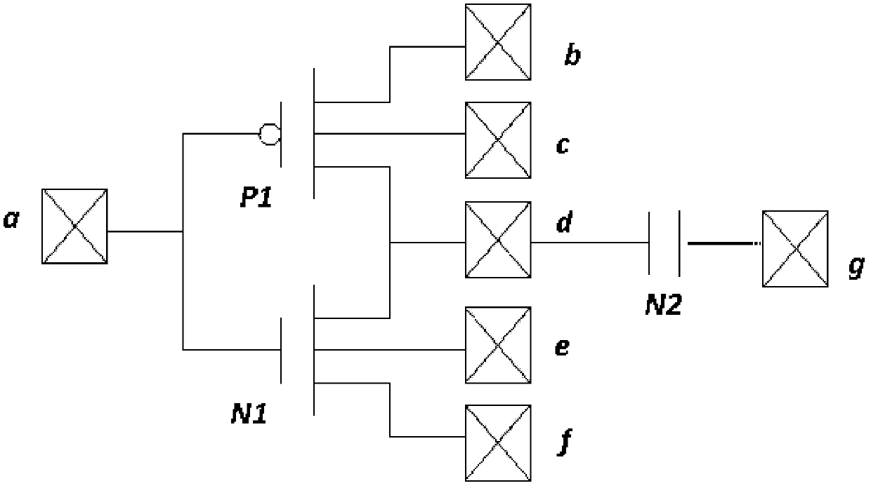
[0012] Such as figure 1 As shown, the test structure of the AC hot carrier injection characteristics of the transistor of the present invention includes: PMOS P1, NMOS N1, and test capacitor N2;

[0013] The gates of P1 and N1 are connected as the test pin a of this test structure; the source of P1 is used as the test pin b of this test structure; the substrate electrode of P1 is used as the test pin c of this test structure; The drain is connected as the test pin d of this test structure; the substrate electrode of N1 is used as the test pin e of this test structure; the source of N1 is used as the test pin f of this test structure; one end of the test capacitor N2 is connected to the test lead Pin d, the other end is grounded as the test pin g of this test structure;

[0014] The charging time of the test load is consistent with the cycle of the AC signal changing from low potential to high potential, its discharge time is consistent with the cycle of AC signal changing fro...


PUM


Abstract

The invention discloses a test structure of transistor alternating current hot carrier injection characteristics. The test structure comprises a PMOS P1 to be tested, an NMOS N1 to be tested and a test load N2. A grid electrode of P1 and a grid electrode of N1 are connected to serve as a test pin a of the test structure, a source electrode of the P1 serves as a test pin b of the test structure, a substrate electrode of the P1 serves as a test pin c of the test structure, a drain electrode of the P1 and a drain electrode of the N1 are connected to serve as a test pin d of the test structure, a substrate electrode of the N1 serves as a test pin e of the test structure, a source electrode of the N1 serves as a test pin of the test structure, one end of the test load N2 is connected with the test pin d, and the other end of the test load N2 is grounded to serve as a test pin g of the test structure. The test structure can accurately simulate the working state of a CMOS in a circuit, can accurately evaluate characteristic changes of the PMOS and the NMOS in the CMOS after the PMOS and the NMOS bear alternating current HCI stress, and can also evaluate characteristic changes of the CMOS after the CMOS bears the alternating current HCI stress.

Description

technical field [0001] The invention relates to the field of semiconductor manufacturing, in particular to a test structure for the AC hot carrier injection characteristics of a transistor. Background technique [0002] The current AC HCI (Hot Carrier Injection, Hot Carrier Injection) test structure is the same as the DC test structure, which is an independent PMOS or NMOS, or a structure with a common substrate electrode or (and) source electrode. When this independent structure is loaded with AC HCI stress, often only AC signals can be applied to one end (gate or drain), and the other end is a DC signal, which cannot truly simulate the working state of CMOS in the circuit, and cannot achieve the best evaluation. Effect. If AC signals are applied to the two ends (gate and drain) of the MOS device through two different devices, it is difficult to control whether the two signals are synchronized, so it is impossible to truly simulate the CMOS working state in the circuit, wh...

Claims


Application Information

Patent Timeline
Patent Type & Authority Applications(China)
IPC IPC(8): G01R31/26H01L23/544
Inventor 沈国飞陈琦曹刚
Owner SHANGHAI HUAHONG GRACE SEMICON MFG CORP
Why Eureka
Try Eureka