Semiconductor structure with stress protection structure and forming method of semiconductor structure

A technology for protecting structures and semiconductors, applied in semiconductor devices, semiconductor/solid-state device manufacturing, semiconductor/solid-state device components, etc., can solve problems such as limiting the integration of semiconductor components, unfavorable advanced process design, and unsuitable components

Active Publication Date: 2013-10-30
NAN YA TECH
View PDF4 Cites 5 Cited by
  • Summary
  • Abstract
  • Description
  • Claims
  • Application Information

AI Technical Summary

Problems solved by technology

Such a complex stress system is not suitable for component setup and can easily lead to component damage
[0006] However, in today's increasingly shrinking integrated circuits, the existence of the peripheral region 104 will inevitably limit the integration of semiconductor elements, which is not conducive to the design of more advanced processes.

Method used


Image

  • Semiconductor structure with stress protection structure and forming method of semiconductor structure
  • Semiconductor structure with stress protection structure and forming method of semiconductor structure
  • Semiconductor structure with stress protection structure and forming method of semiconductor structure

Examples


Embodiment Construction

[0025] In order to enable those skilled in the art to which the present invention belongs to further understand the present invention, the following description lists several preferred embodiments of the present invention, together with the accompanying drawings and descriptions, to explain in detail the content of the present invention and the effects to be achieved. .

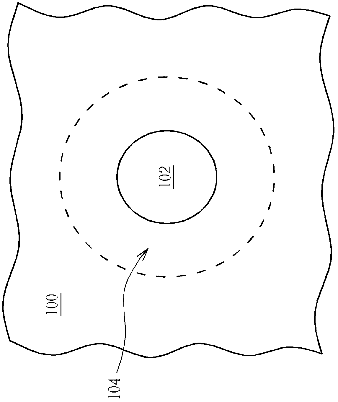
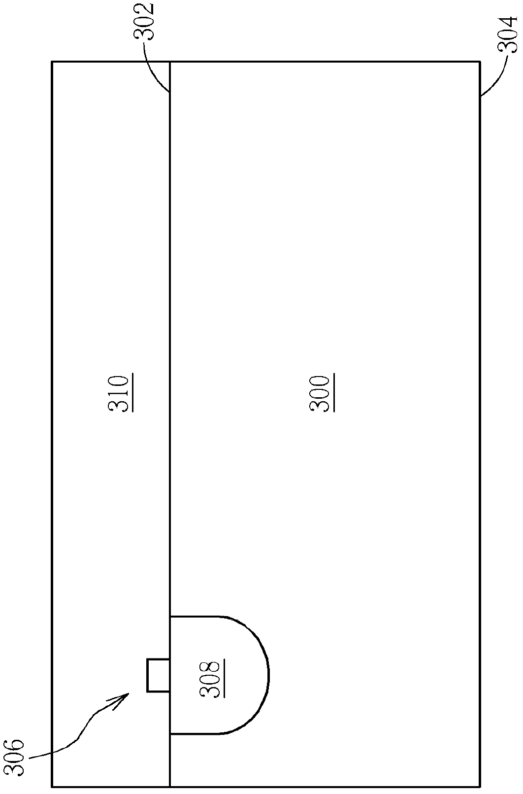
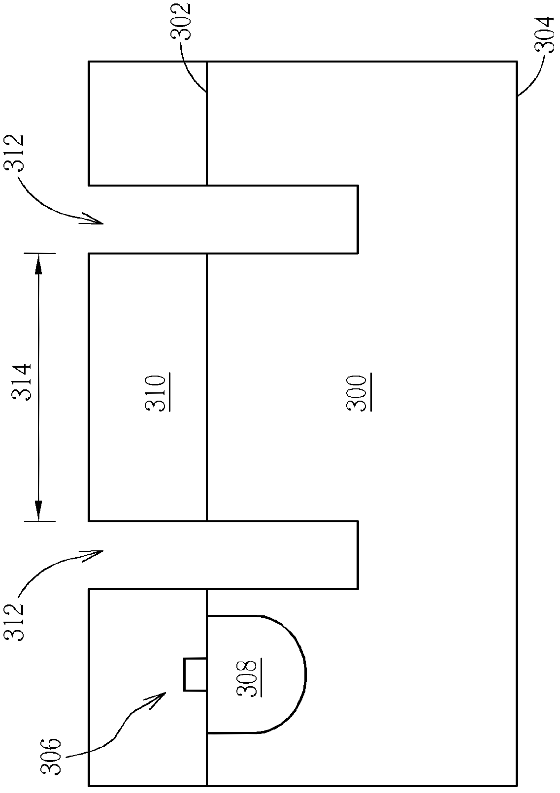
[0026] In order to overcome the aforementioned problem of complex stress near the through silicon via, the present invention forms a stress protection structure around the through silicon via, which has a sealed air space and surrounds the through silicon via. Please refer to Figure 2 to Figure 8 , Which is a schematic diagram showing the steps of forming a semiconductor structure with a stress protection structure according to the present invention. Such as figure 2 As shown, first, a substrate 300 is provided, such as a silicon substrate, an epitaxial silicon substrate, a silicon germanium substrate, a silic...


PUM


Abstract

The invention discloses a semiconductor structure with a stress protection structure. The semiconductor structure includes a substrate, a stress generating element and a stress protection device. The substrate is provided with a first surface and a second surface which are in relative arrangement. The stress generating element is disposed in the substrate. The stress protection structure is disposed on a side of the first surface of the substrate, and surrounds the stress protection structure which is provided with a sealed air space inside. The invention also provides a forming method of the semiconductor structure with the stress protection structure.

Description

Technical field [0001] The invention relates to a semiconductor structure with a stress protection structure and a method for forming the same. In particular, the stress protection structure has a closed air space and can provide a stress buffer effect. Background technique [0002] In the modern information society, micro-processing systems composed of integrated circuits (IC) have long been widely used in all aspects of life, such as automatically controlled household appliances, mobile communication equipment, personal computers, etc., are integrated The use of circuits. With the increasing advancement of science and technology, as well as the various imaginations of human society for electronic products, integrated circuits are also developing in the direction of more diversification, more precision, and smaller size. [0003] Generally, integrated circuits are formed by dies produced in existing semiconductor processes. The process of manufacturing a die starts with the prod...

Claims


Application Information

Patent Timeline
IPC IPC(8): H01L23/48H01L21/768
Inventor 陈逸男徐文吉叶绍文刘献文
Owner NAN YA TECH
Why Eureka
Try Eureka