MEMS (Micro-Electro-Mechanical System) device, manufacturing method thereof and electronic device

A technology for electronic devices and MEMS patterns, which is applied in the manufacture of microstructure devices, microstructure devices, semiconductor/solid-state device components, etc., can solve problems such as fragmentation, easy breakage, and wafer fragility, so as to reduce process costs and increase service life , the effect of reducing the probability of fragmentation

Active Publication Date: 2016-05-11
SEMICON MFG INT (SHANGHAI) CORP
View PDF12 Cites 1 Cited by
  • Summary
  • Abstract
  • Description
  • Claims
  • Application Information

AI Technical Summary

Problems solved by technology

[0006] Deep etching is often used in the preparation process of MEMS devices. Some products are very thin, and some deep holes are etched on the thin wafer (wafer), which makes the Wafer very fragile and easy to break.
The problem of fragmentation will occur when doing the WaferMount process of such MEMS products

Method used


Image

  • MEMS (Micro-Electro-Mechanical System) device, manufacturing method thereof and electronic device
  • MEMS (Micro-Electro-Mechanical System) device, manufacturing method thereof and electronic device
  • MEMS (Micro-Electro-Mechanical System) device, manufacturing method thereof and electronic device

Examples


preparation example Construction

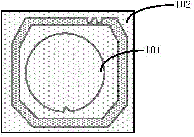
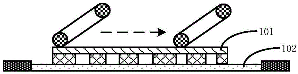
[0039] Because deep etching is often used in the preparation process of MEMS devices, there are many deep grooves in the MEMS wafer, such as Figure 1a As shown in the figure on the right, some products are very thin, which makes the wafer very fragile and easy to break, such as Figure 1d The position indicated by the arrow. The problem of fragmentation will occur when doing the WaferMount process of such MEMS products.

[0040]Therefore, it is necessary to further improve the cutting method of the current MEMS wafer in order to eliminate the above-mentioned problems.

Embodiment 1

[0042] In order to solve the problems existing in the prior art, the present invention provides a kind of preparation method of MEMS device, below in conjunction with attached Figure 2a-2d The method is described further.

[0043] First, step 201 is performed to provide a MEMS wafer 201 on which MEMS patterns are formed.

[0044] Specifically, such as Figure 2a As shown, the MEMS wafer 201 can be made of semiconductor materials such as silicon, polysilicon or SiGe, and is not limited to a certain one.

[0045] The MEMS device formed in the present invention may be a sensor, such as a pressure sensor, an acceleration sensor, etc., or a MEMS microphone, or other types of MEMS devices, and is not limited to a certain one.

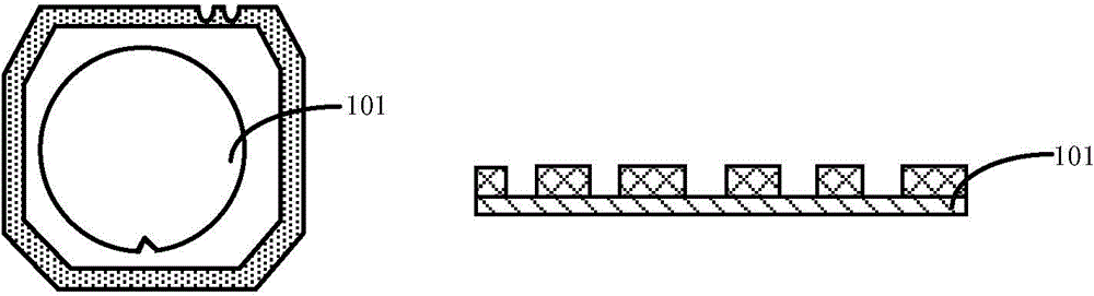
[0046] Wherein, the MEMS pattern includes deep holes and / or deep grooves, such as Figure 2a As shown in the figure on the right, the pattern is not limited to this example, and other patterns may be formed.

[0047] Then the MEMS wafer 201 forming the M...

Embodiment 2

[0067] In order to solve the problems existing in the prior art, the present invention provides a kind of preparation method of MEMS device, below in conjunction with attached Figures 3a-3d The method is described further.

[0068] First, step 301 is performed to provide a MEMS wafer 301 on which MEMS patterns are formed.

[0069] Specifically, such as Figure 3a As shown, the MEMS wafer 301 can be made of semiconductor materials such as silicon, polysilicon or SiGe, and is not limited to a certain one.

[0070] The MEMS device formed in the present invention may be a sensor, such as a pressure sensor, an acceleration sensor, etc., or a MEMS microphone, or other types of MEMS devices, and is not limited to a certain one.

[0071] Wherein, the MEMS pattern includes deep holes and / or deep grooves, such as Figure 3a As shown in the figure on the right, the pattern is not limited to this example, and other patterns may be formed.

[0072] Then the MEMS wafer 301 forming the ...


PUM


Abstract

The invention relates to an MEMS (Micro-Electro-Mechanical System) device, a manufacturing method thereof and an electronic device. The method comprises the following steps: S1, providing an MEMS wafer, wherein MEMS patterns are formed on a front side of the MEMS wafer; S2, forming an adhesive tape on the front side of the MEMS wafer in order to cover the MEMS patterns; and S3, reversing the MEMS wafer, arranging a stress protection layer on a back side of the MEMS wafer, and applying a pressure to the stress protection layer in order to bond the MEMS wafer and the adhesive tape. The manufacturing method has the advantages that 1, the wafer breakage probability is lowered, and the service life of a machine stand is prolonged; 2, the yield is increased, and the process cost is lowered; and 3, property insurance normal production is maintained, and the yield is increased.

Description

technical field [0001] The invention relates to the field of semiconductors, in particular, the invention relates to a MEMS device, a preparation method thereof, and an electronic device. Background technique [0002] For the increasing demand for high-capacity semiconductor storage devices, the integration density of these semiconductor storage devices has attracted people's attention. In order to increase the integration density of semiconductor storage devices, many different methods have been adopted in the prior art, such as by reducing the wafer size. And / or change the internal structure unit to form multiple memory units on a single wafer. For the method of increasing the integration density by changing the unit structure, attempts have been made to reduce the unit area. [0003] In the field of electronic consumption, multi-function devices are more and more popular among consumers. Compared with devices with simple functions, the production process of multi-functio...

Claims


Application Information

Patent Timeline
IPC IPC(8): B81B7/02B81C1/00
Inventor 郑超李卫刚刘炼王伟
Owner SEMICON MFG INT (SHANGHAI) CORP
Why Eureka
Try Eureka