Thin-film transistor device and method for manufacturing same, organic electroluminescent display element, and organic electroluminescent display device

A technology of thin-film transistors and devices, applied in semiconductor/solid-state device manufacturing, transistors, electric solid-state devices, etc., can solve problems such as poor electrical connections

Active Publication Date: 2013-10-30
PANASONIC CORP
View PDF5 Cites 0 Cited by
  • Summary
  • Abstract
  • Description
  • Claims
  • Application Information

AI Technical Summary

Problems solved by technology

[0009] However, the TFT device related to the prior art has the following problem: the organic semiconductor layer is formed to the part where the organic semiconductor

Method used


Image

  • Thin-film transistor device and method for manufacturing same, organic electroluminescent display element, and organic electroluminescent display device
  • Thin-film transistor device and method for manufacturing same, organic electroluminescent display element, and organic electroluminescent display device
  • Thin-film transistor device and method for manufacturing same, organic electroluminescent display element, and organic electroluminescent display device

Examples


Embodiment approach 1

[0131] 1. Overall structure of the organic EL display device 1

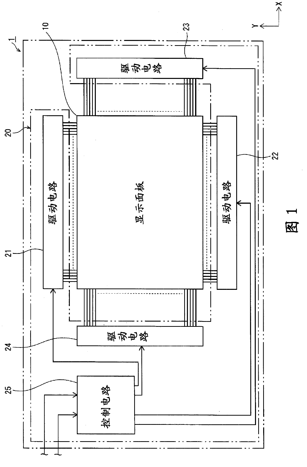
[0132] Below, use figure 1 The structure of the organic EL display device 1 according to Embodiment 1 of the present invention will be described.

[0133] Such as figure 1 As shown, the organic EL display device 1 is configured to include an organic EL display panel 10 and a drive control circuit unit 20 connected thereto.

[0134] The organic EL display panel 10 is a panel utilizing the electroluminescence phenomenon of organic materials, and is configured such that a plurality of organic EL elements are arranged in a matrix, for example. The drive control circuit unit 20 includes a control circuit 25 and four drive circuits 21 to 24 .

[0135] In the organic EL display device 1 according to this embodiment, the arrangement of the drive control circuit unit 20 with respect to the organic EL display panel 10 is not limited to this.

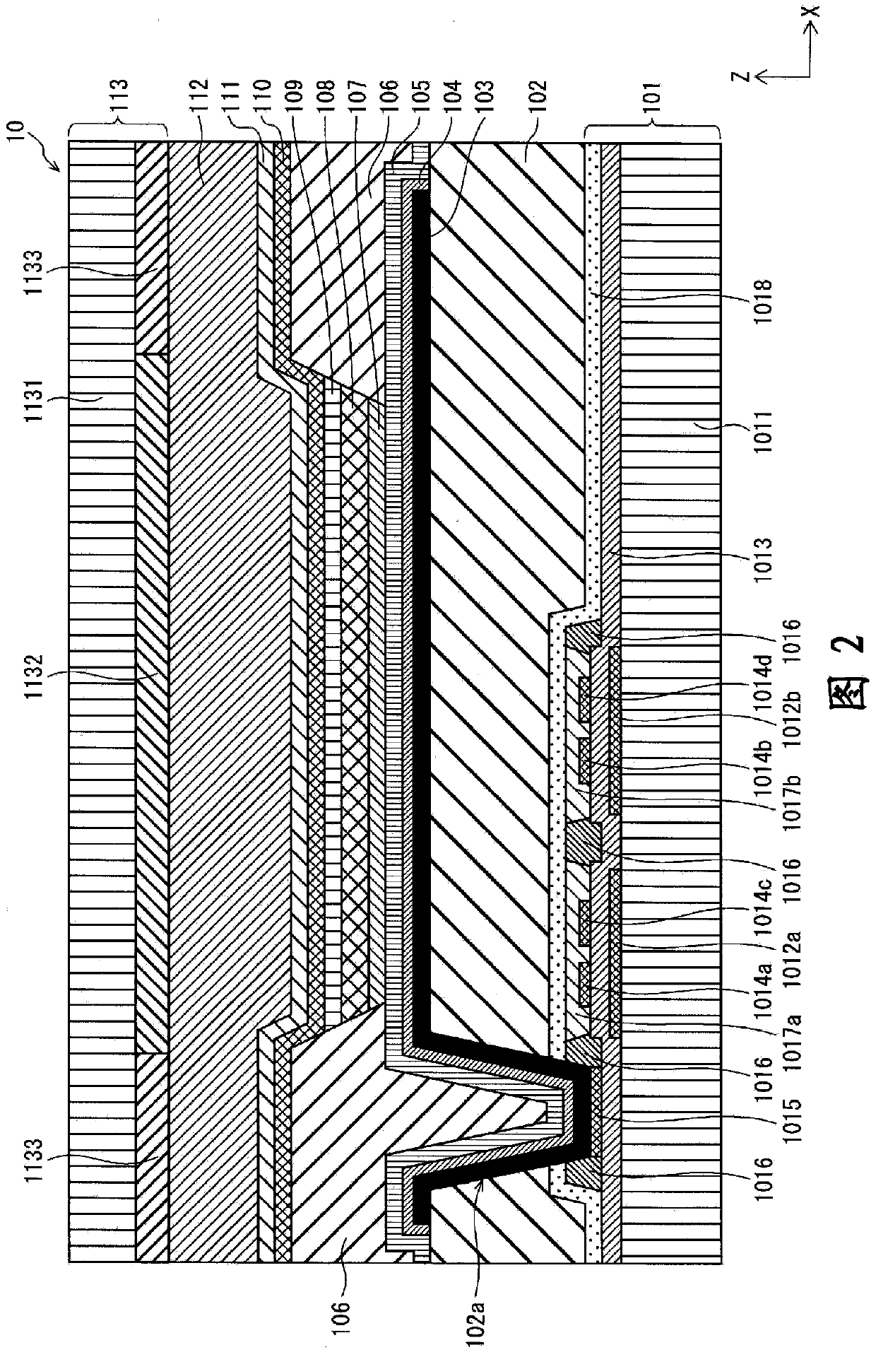
[0136] 2. Structure of the organic EL display panel 10

[0137] use fig...

Embodiment approach 2

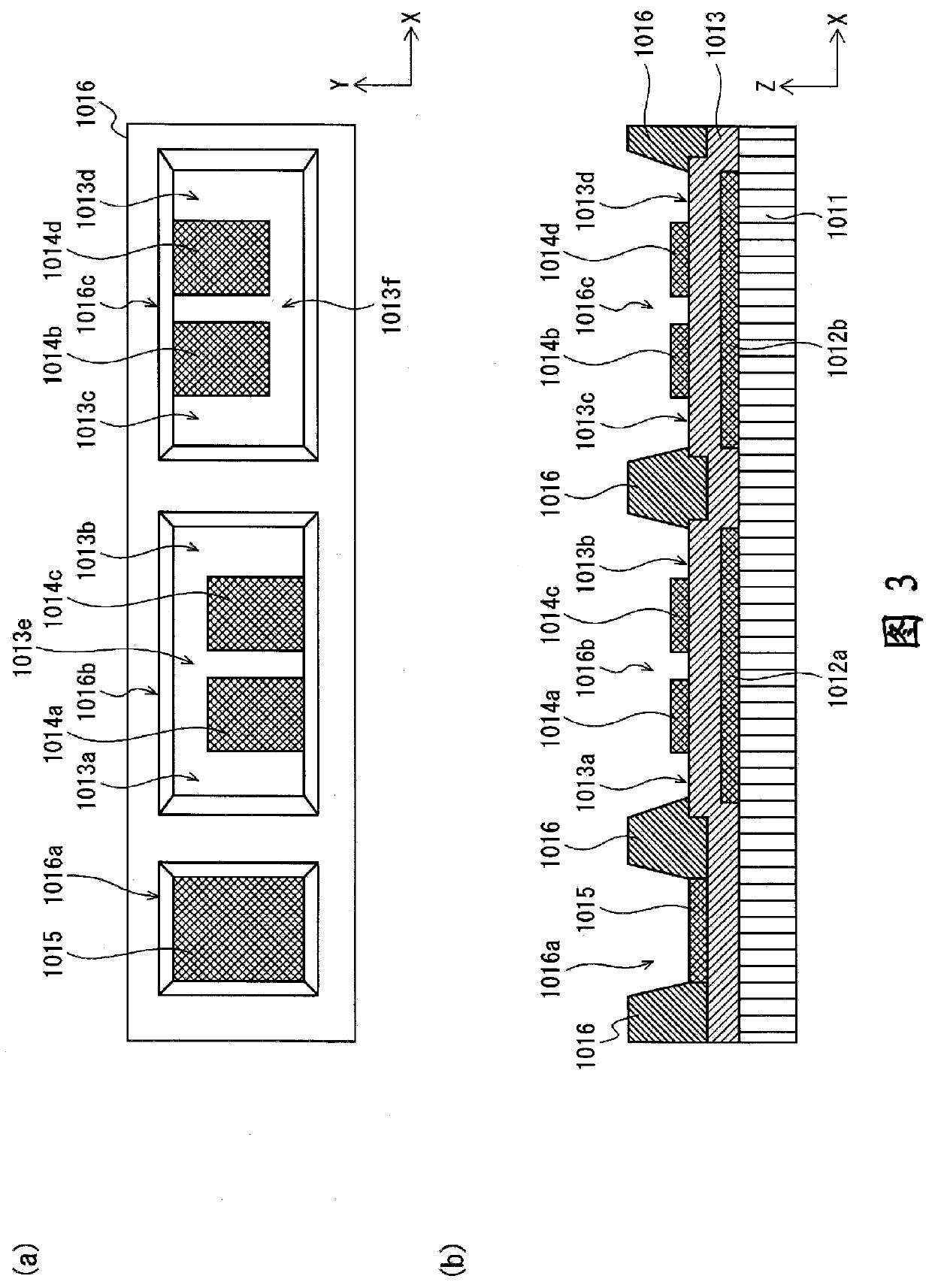
[0245] use Figure 9 (a) The structure of the TFT substrate according to Embodiment 2 of the present invention will be described. Figure 9 (a) is the same as in Embodiment 1 above image 3 Figures corresponding to (a) and other configurations are the same as those in Embodiment 1 described above, so illustration and description thereof are omitted.

[0246] Such as Figure 9 As shown in (a), in the TFT substrate according to this embodiment, four openings 2016 a , 2016 b , 2016 c , and 2016 d are defined by the partition wall 2016 . Among them, the connection wirings 2015a and 2015d are arranged at the bottom of the openings 2016a and 2016d, respectively, and do not function as channel parts.

[0247] Furthermore, in this embodiment, if Figure 9 As shown in (a), neither the opening portion 2016a nor the opening portion 2016d functions as a channel portion, but one opening portion, for example, the opening portion 2016d belongs to the TFT element corresponding to the adja...

Embodiment approach 3

[0254] use Figure 9 (b) The structure of the TFT substrate according to Embodiment 3 of the present invention will be described. also, Figure 9 (b) is the same as that in Embodiment 1 above image 3 The diagram corresponding to (a) and other configurations are the same as those of Embodiments 1 and 2 above, so illustration and description thereof will be omitted.

[0255] Such as Figure 9 As shown in (b), in the TFT substrate according to this embodiment, four openings 3016 a , 3016 b , 3016 c , and 3016 d are defined by the partition wall 3016 . Among them, the connection wirings 3015a and 3015d are arranged at the bottom of the openings 3016a and 3016d, respectively, and do not function as channel parts.

[0256] Furthermore, in this embodiment, if Figure 9 As shown in (b), neither the opening portion 3016a nor the opening portion 3016d functions as a channel portion, but one opening portion, for example, the opening portion 3016d belongs to a TFT corresponding to a...


PUM


Abstract

In a thin film transistor device, partition walls define first, second, and third apertures. In plan view, at a bottom portion of the first aperture, a center of a total of areas of a source electrode portion and a drain electrode portion is offset from a center of area of the bottom portion in a direction differing from a direction of the third aperture, and at a bottom portion of one of the first and second apertures, a center a total of areas of a source electrode portion and a drain electrode portion is offset from a center of area of the bottom portion in a direction differing from a direction of the other one of the first and second apertures.

Description

technical field [0001] The invention relates to a thin film transistor device and its manufacturing method, an organic EL display element and an organic EL display device. Background technique [0002] In liquid crystal display panels and organic EL display panels, thin film transistor devices (devices) in which thin film transistor (TFT (Thin Film Transistor)) elements are formed for each sub-pixel are used in order to control light emission on a sub-pixel basis. And, especially, the development of thin film transistor devices using organic semiconductor materials as semiconductor layers has been progressing. [0003] Such as Figure 14 As shown in (a), the organic TFT device related to the prior art, for example, is sequentially stacked on a substrate 9011 with gate electrodes 9012a, 9012b, an insulating layer 9013, source electrodes 9014a, 9014b, drain electrodes (not shown) and an organic semiconductor layer. 9017a, 9017b. The organic semiconductor layers 9017a and 901...

Claims


Application Information

Patent Timeline
IPC IPC(8): H01L21/336G09F9/00G09F9/30H01L27/32H01L29/786H01L51/50
CPCH01L27/3262H01L27/3248H01L27/3274H01L27/1292H01L51/0545H01L29/78693H01L29/66742H01L27/1225H01L51/52H01L51/105H10K59/123H10K59/125H10K59/1213H10K10/84H10K10/466H10K50/80
Inventor 奥本有子宫本明人受田高明
Owner PANASONIC CORP
Why Eureka
Try Eureka