inductance

A technology of inductance and inductance coil, applied in the field of inductance, can solve the problems of increasing parasitic capacitance and reducing resonance frequency, etc., and achieve the effect of reducing parasitic capacitance, improving quality factor and increasing cost

Active Publication Date: 2016-02-10
SHANGHAI HUAHONG GRACE SEMICON MFG CORP
View PDF5 Cites 0 Cited by
  • Summary
  • Abstract
  • Description
  • Claims
  • Application Information

AI Technical Summary

Problems solved by technology

But the shortcoming of existing second kind of inductance is, because the concentration of N well 12 is much higher than P-type semiconductor substrate 11, will form extra between the N well 12 that forms on P-type semiconductor substrate 11 and inductance coil 13 The parasitic capacitance increases the parasitic capacitance between the inductance coil 13 and the P-type semiconductor substrate 11, which offsets some of the improved quality factors to a certain extent, and also reduces the resonant frequency

Method used


Image

  • inductance
  • inductance
  • inductance

Examples


Embodiment Construction

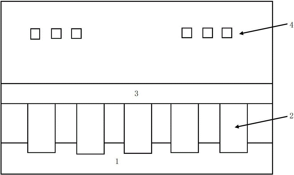
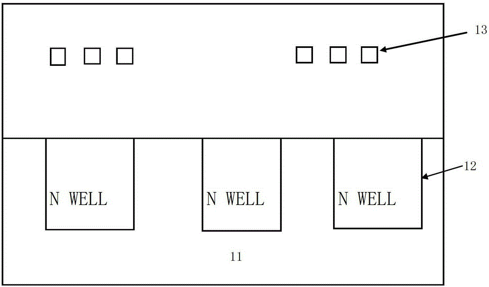
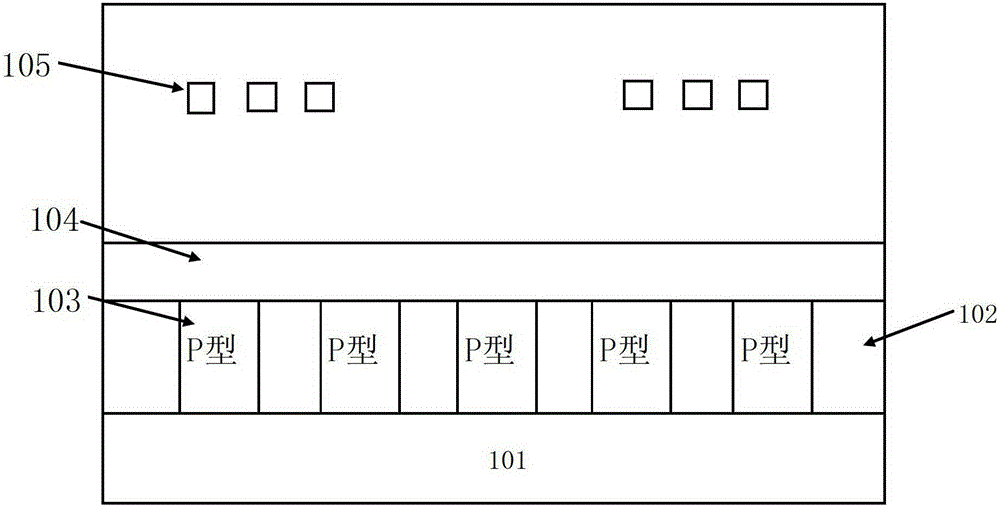
[0028] like image 3 Shown is a schematic cross-sectional structure diagram of an inductor according to Embodiment 1 of the present invention. Embodiment 1 of the present invention includes an inductor coil 105 and a substrate structure. The inductor coil 105 is a single-ended inductor, a differential inductor, a laminated inductor or a transformer. The inductance coil 105 is located above the substrate structure, and the inductance coil 105 and the substrate structure are separated by an insulating dielectric layer 107, and the insulating dielectric layer 107 in Embodiment 1 of the present invention is a silicon oxide layer .

[0029] The substrate structure includes:

[0030] A P-type semiconductor substrate 101.

[0031] An N-type epitaxial layer 102 formed on the semiconductor substrate 101 .

[0032] A plurality of P-type doped regions 103 in a strip structure, each of which is an ion implantation region defined by a photolithography process, the formation of each of...


PUM


Abstract

The invention discloses an inductor. The inductor comprises an inductance coil and a substrate structure. The substrate structure comprises a P-type semiconductor substrate, an N-type epitaxial layer and a plurality of P-type doped regions of bar-type structures, wherein the P-type doped regions are formed by adopting the photoetching and ion implantation technology. The depth of the P-type doped regions is larger than or equal to the thickness of the N-type epitaxial layer. The P-type doped regions divide the N-type epitaxial layer into a plurality of N-type doped regions to form a structure that the N-type doped regions and the P-type doped regions are alternately arranged. An exhaustion region is formed in the substrate by the N-type doped regions and the P-type doped regions which are alternately arranged to enable the substrate to be in a high resistance state so that the eddy of the substrate can be blocked. The stray capacitance of the substrate can be reduced through the exhaustion region, and quality factors of the indicator can be improved. According to the indicator, the deep groove isolation technology is not needed, and technology cost is low.

Description

technical field [0001] The invention relates to a semiconductor integrated circuit, in particular to an inductor. Background technique [0002] In semiconductor integrated circuits, such as radio frequency devices, inductors are often used, and the inductors are integrated with other semiconductor devices in the same semiconductor substrate. In the prior art, the inductor is generally formed on a semiconductor substrate, such as a silicon substrate, and is separated from the semiconductor substrate by an insulating dielectric layer. When the inductor is connected to a current, a magnetic field will be generated, and the magnetic field of the inductor will pass through the semiconductor substrate vertically, and form an eddy current on the semiconductor substrate, especially the surface of the semiconductor substrate, which is opposite to the metal current direction of the upper inductor. The eddy current will not only bring eddy current loss, but also generate an induced ma...

Claims


Application Information

Patent Timeline
Patent Type & Authority Patents(China)
IPC IPC(8): H01L23/522
Inventor 黄景丰
Owner SHANGHAI HUAHONG GRACE SEMICON MFG CORP
Why Eureka
Try Eureka