Light-emitting element spot measurement machine

A technology of light-emitting element and spot measuring machine, which is applied in photometry, optical radiation measurement, measuring device, etc., can solve the problem that the light transmittance of the scattering angle carrier plate affects the efficiency of light receiving, the result of the light-emitting diode 21 is inaccurate, and cannot be used. Problems such as point measurement of the object to be measured

Inactive Publication Date: 2013-11-27
致茂电子(苏州)有限公司
View PDF8 Cites 3 Cited by
  • Summary
  • Abstract
  • Description
  • Claims
  • Application Information

AI Technical Summary

Problems solved by technology

Those who are familiar with this technology know that the known method of the wafer tray 2 is to use the blue film to spread it out, place the wafer to be tested on the blue film, and then place it on a carrier plate for spot measurement, or directly place it Work on the carrier plate, regardless of the above methods, because there are obstacles under the object to be tested, which only limit the specific form of the object to be tested that emits light upwards, and cannot be used for the point of the object to be measured that emits light from both sides Measurement
[0004] Also, please refer to Figure 11 , is a representative diagram of China Taiwan Invention Patent Application Publication No. 201109635A1, the object to be tested, i.e. light-emitting diode 21, is placed on a transparent carrier board 20, however, the light-emitting diode 21 emits downward during the test The light is transmitted through the transparent carrier plate 20 made of transparent material. Since the light that passes through the medium of the transparent carrier plate 20, the light emitted downward will deviate from its scattering angle, and the factor of the light transmittance of the carrier plate will also affect the light collection. Efficiency, especially when the lower light detection device 40 is the light entrance of the integrating sphere 41 must be accurately calculated, the result of the detected LED 21 will be inaccurate

Method used


Image

  • Light-emitting element spot measurement machine
  • Light-emitting element spot measurement machine
  • Light-emitting element spot measurement machine

Examples


Embodiment Construction

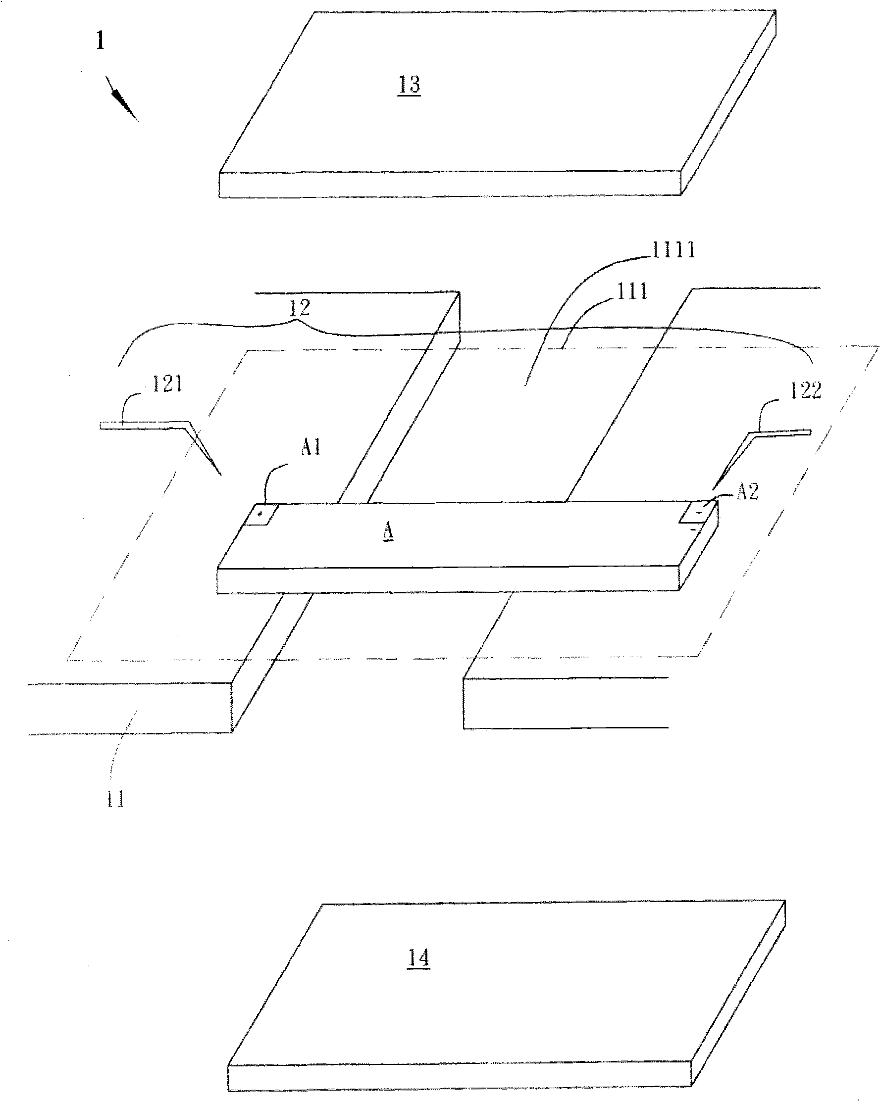
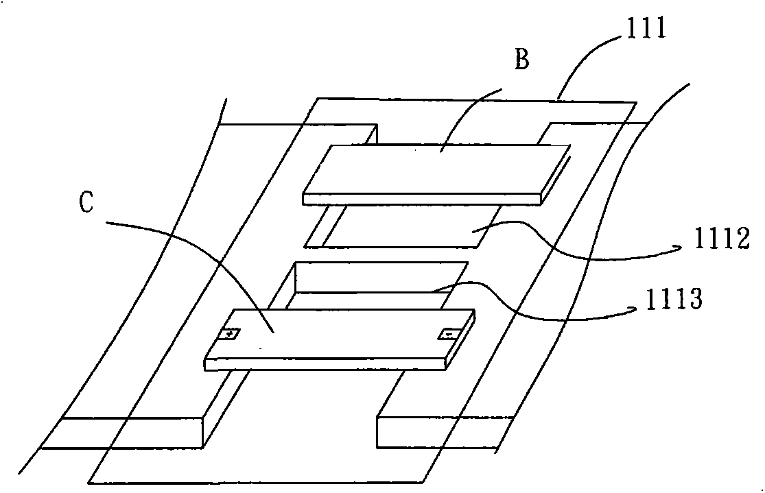
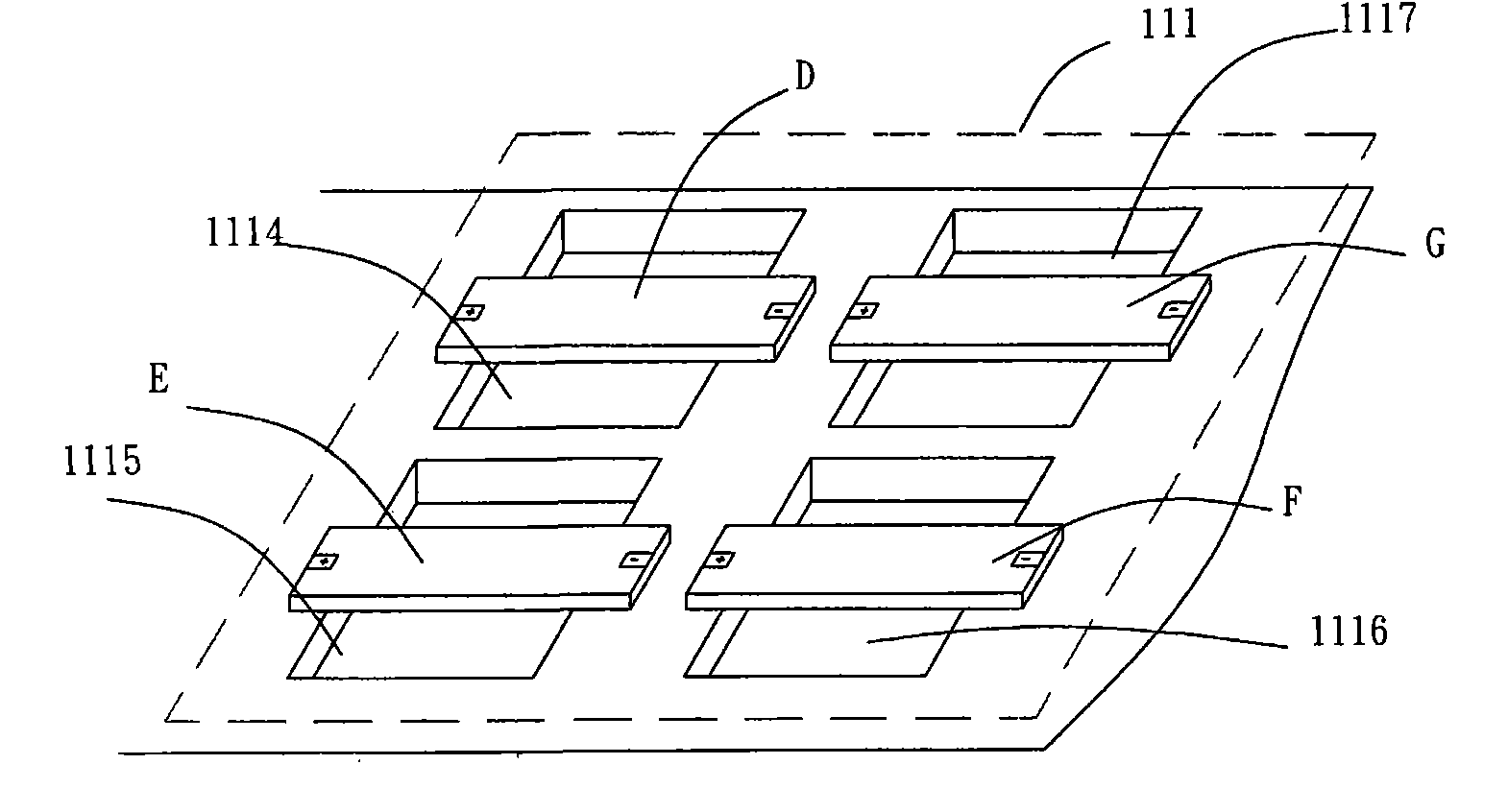
[0020] Please refer to figure 1 , is a three-dimensional schematic diagram of a first aspect of a first preferred embodiment of a spot testing machine for light-emitting elements of the present invention. Light-emitting element point test machine 1, through applying electricity to make a light-emitting element A turn on and emit light, and then collect optical data of the light-emitting element A, including: a carrying platform 11, with a carrying position 111 forming a spanning space 1111 , the straddling space 1111 of the carrying position 111 is used to hold at least one light-emitting element A; a set of probes 12 includes a first probe 121 and a second probe 122 for contacting a first probe of the light-emitting element A An electrode A1 and a second electrode A2, and provide the required electrical properties, so that the contacted light-emitting element A is turned on and emits light; a first light collection device 13 is correspondingly arranged above the carrying pla...


PUM


Abstract

The invention discloses a light-emitting element spot measurement machine. Electrical properties are applied to make light-emitting elements be connected and emit light, and then the optical property data of the light-emitting elements are collected. The light-emitting element spot measurement machine comprises a bearing platform, a set of probes, a first optical property collecting device and a second optical property collecting device, wherein the bearing platform is provided with a bearing position for forming a spanning and erecting space which is used for bearing and placing at least one light-emitting element; the probes make contact with the light-emitting elements and provide the electrical properties needing applying; the first optical property collecting device is correspondingly arranged above the bearing platform and collects light upwards emitted by the light-emitting elements after being connected; the second optical property collecting device is correspondingly arranged below the bearing platform and collects light downwards emitted by the light-emitting elements after being connected. The second optical property collecting device can be also replaced by an optical property reflecting device which is used for reflecting the light downwards emitted by the light-emitting elements to the first optical property collecting device. According to the light-emitting element spot measurement machine, the light downwards emitted by the light-emitting elements can be made to directly enter a light collector without transmitting through a bearing body, so that the detecting result is prevented from being affected by the factors of light transmittance, the change of light marching angles and the like.

Description

technical field [0001] The present invention relates to a light-emitting element point measuring machine, especially a bearing position that provides a straddling space, so that the light emitted by the light-emitting element can enter the light collector without passing through the carrier. Spot testing machine for light-emitting elements. Background technique [0002] Please refer to Figure 10 , is a representative diagram of China Taiwan Invention Patent Application Publication No. 201133695A1. As shown in the figure, a wafer carrying and fixing device includes a frame body 31 and a plurality of fixing units 32; the fixing units 32 are arranged on one side of the frame body 31, and each fixing unit 32 includes a pivot 321, a pivot arm 322 and a limit portion 323; the pivot arm 322 is pivotally connected to the frame body 31 through the pivot shaft 321, and is magnetically adsorbed to the frame body 31; wherein, a crystal placed on the frame body 31 The disk 2 can be at...

Claims


Application Information

Patent Timeline
Patent Type & Authority Applications(China)
IPC IPC(8): G01J1/04
Inventor 高宏达张敏宏
Owner 致茂电子(苏州)有限公司
Why Eureka
Try Eureka