PN step of LED (Light Emitting Diode) chip, LED chip and manufacturing method of PN step

A technology of LED chips and manufacturing methods, which is applied in the direction of electrical components, circuits, semiconductor devices, etc., can solve the problems of reducing the light output effect of LED chips, the drop of LED chip turn-on voltage, and poor coverage effects, so as to increase the effective coverage area and reduce leakage. Current, the effect of increasing the turn-on voltage

Active Publication Date: 2013-11-27
JUCAN PHOTOELECTRIC TECH (SUQIAN) CO LTD
View PDF5 Cites 4 Cited by
  • Summary
  • Abstract
  • Description
  • Claims
  • Application Information

AI Technical Summary

Problems solved by technology

[0003] However, see figure 1 As shown, the connection surface between the upper step surface 110 and the lower step surface 120 of the PN step 100a in the existing LED chip epitaxial layer 100 (collectively referred to as the PN step side 130 herein) is perpendicular to the upper step surface 110 and the lower step surface 120 Or substantially vertical, resulting in the inability to

Method used


Image

  • PN step of LED (Light Emitting Diode) chip, LED chip and manufacturing method of PN step
  • PN step of LED (Light Emitting Diode) chip, LED chip and manufacturing method of PN step
  • PN step of LED (Light Emitting Diode) chip, LED chip and manufacturing method of PN step

Examples


Embodiment 1

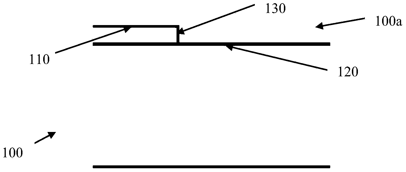
[0042] See figure 2 As shown, a PN step of an LED chip. The LED chip (not shown) includes a substrate and an epitaxial layer 200 formed on the substrate. The epitaxial layer 200 includes an N-type conductive layer, a light-emitting layer, and a P-type conductive layer ( The drawings in this paper are not specifically divided and shown), the epitaxial layer 200 has a PN step 200a, the PN step 200a is covered with an insulating passivation film 300, the upper step surface 210 of the PN step 200a is a P-type conductive layer, and the lower step surface 220 is an N-type conductive layer, and the connection between the upper stepped surface 210 and the lower stepped surface 220 forms a PN stepped side surface 230;

[0043] Wherein, the PN step side 230 includes a first connection side on the upper step surface 210 and a second connection side on the lower step surface 220, the second connection side is located between the first connection side and the end of the lower step surface...

Embodiment 2

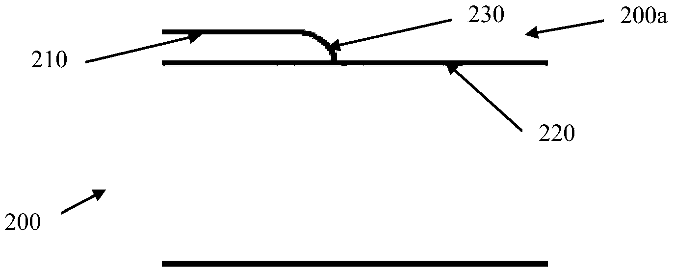
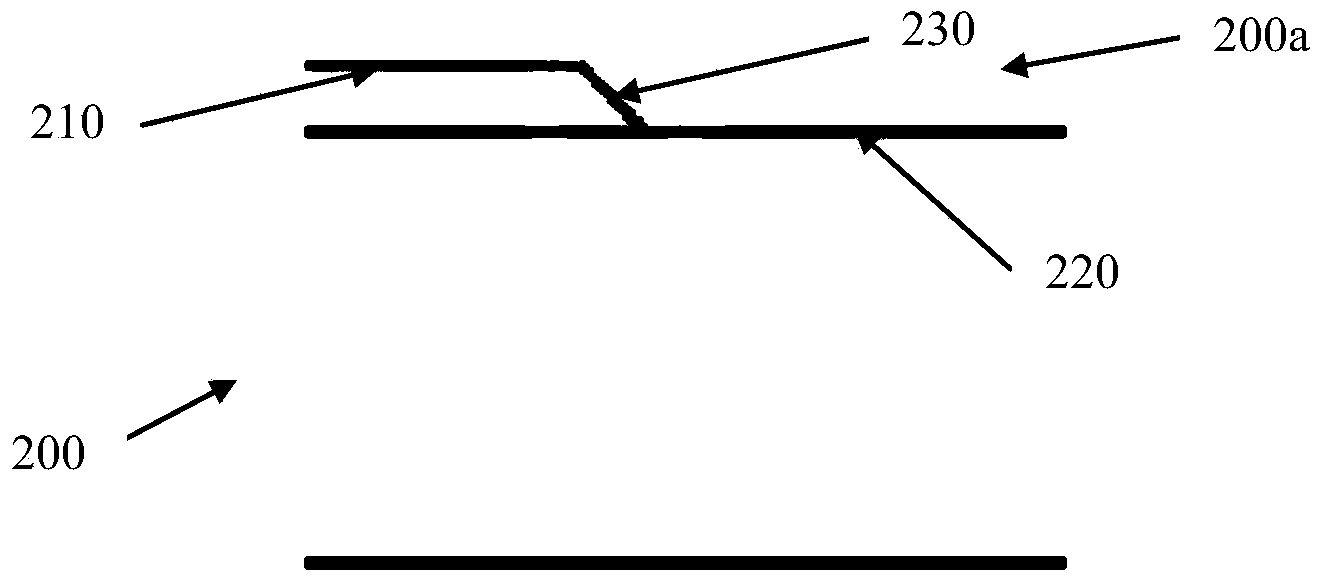
[0056] See image 3 As shown, a PN step of an LED chip, the LED chip includes a substrate and an epitaxial layer 200 formed on the substrate, the epitaxial layer 200 sequentially includes an N-type conductive layer, a light emitting layer and a P-type conductive layer, and the epitaxial layer 200 has a PN The step 200a, the PN step 200a is covered with an insulating passivation film 300, the upper step surface 210 of the PN step 200a is a P-type conductive layer, and the lower step surface 220 is an N-type conductive layer, and the upper step surface 210 and the lower step surface 220 The inter-connection forms the PN step side 230;

[0057] Wherein, the PN step side 230 includes a first connection side on the upper step surface 210 and a second connection side on the lower step surface 220, the second connection side is located between the first connection side and the end of the lower step surface 220, and the PN The side surface 230 of the step is a slope, preferably, the ...

Embodiment 3

[0062] An LED chip, comprising a substrate, an epitaxial layer 200 formed on the substrate and consisting of an N-type conductive layer, a light-emitting layer and a P-type conductive layer, an N-type electrode electrically connected to the N-type conductive layer, and an N-type electrode electrically connected to the P-type conductive layer. P-type electrodes electrically connected to the conductive layer, see Figure 5 As shown, the epitaxial layer 200 has a PN step, and the PN step 200a is covered with an insulating passivation film 300 , wherein the PN step adopts the PN step 200a as described in Embodiment 1 or Embodiment 2. Specifically, the insulating passivation film 300 may be covered on the PN step 200a by using a deposition method or other known methods.

[0063] In order to facilitate the description of the core technical points and technical effects of the present invention, this patent Figure 5 The shown insulating passivation film 300 is directly covered on th...


PUM

PropertyMeasurementUnit
Thicknessaaaaaaaaaa
Thicknessaaaaaaaaaa

Abstract

The invention discloses a PN step of an LED (Light Emitting Diode) chip, the LED chip and a manufacturing method of the PN step. The LED chip comprises a substrate and an epitaxial layer which is formed on the substrate, wherein the epitaxial layer is provided with the PN step, the PN step is covered with an insulation passive film, the upper step surface of the PN step is a P type conducting layer, the lower step surface of the PN step is an N type conducting layer, and a PN step side surface is formed in a way that the upper step surface and the lower step surface are connected; the PN step side surface comprises a first connecting edge which is positioned on the upper step surface and a second connecting edge which is positioned on the lower step surface, the second connecting edge is positioned between the first connecting edge and the end part of the lower step surface, and the PN step side surface is a curved surface or an inclined surface. According to the PN step of the LED chip, the LED chip and the manufacturing method, which are disclosed by the invention, the covering effect of the insulation passive film on the LED chip is facilitated, the turn-on voltage of the LED chip is effectively increased, the leak current is reduced, and the luminous efficiency of the LED chip is effectively increased at the same time.

Description

technical field [0001] The invention relates to a manufacturing technology of an LED chip, in particular to a PN step of the LED chip, the LED chip and a manufacturing method. Background technique [0002] The manufacturing process of the conventional LED chip is mainly as follows: firstly, the N-type conductive layer, the light-emitting layer and the P-type conductive layer are sequentially deposited on the substrate (the existing sapphire material is mainly used), among which, the N-type conductive layer, the light-emitting layer and the P-type The conductive layer constitutes the epitaxial layer (GaN material is mainly used at present), and steps are formed on the epitaxial layer by etching (generally using photolithography) (herein collectively referred to as PN steps), which makes part of the N-type conductive layer of the epitaxial layer The surface is exposed, that is, the upper step surface of the step is a P-type conductive layer, and the lower step surface is an N-...

Claims


Application Information

Patent Timeline
IPC IPC(8): H01L33/02H01L33/00
Inventor 魏天使李忠武何金霞
Owner JUCAN PHOTOELECTRIC TECH (SUQIAN) CO LTD
Why Eureka
Try Eureka