

photoelectric conversion device
A photoelectric conversion device and circuit board technology, which is applied in the coupling of optical waveguides, etc., can solve the problems of low assembly efficiency and low product yield, and achieve the effects of simple assembly method, improved product yield, and improved assembly efficiency
- Summary
- Abstract
- Description
- Claims
- Application Information
AI Technical Summary
Problems solved by technology
Method used
Image

Examples
Embodiment Construction
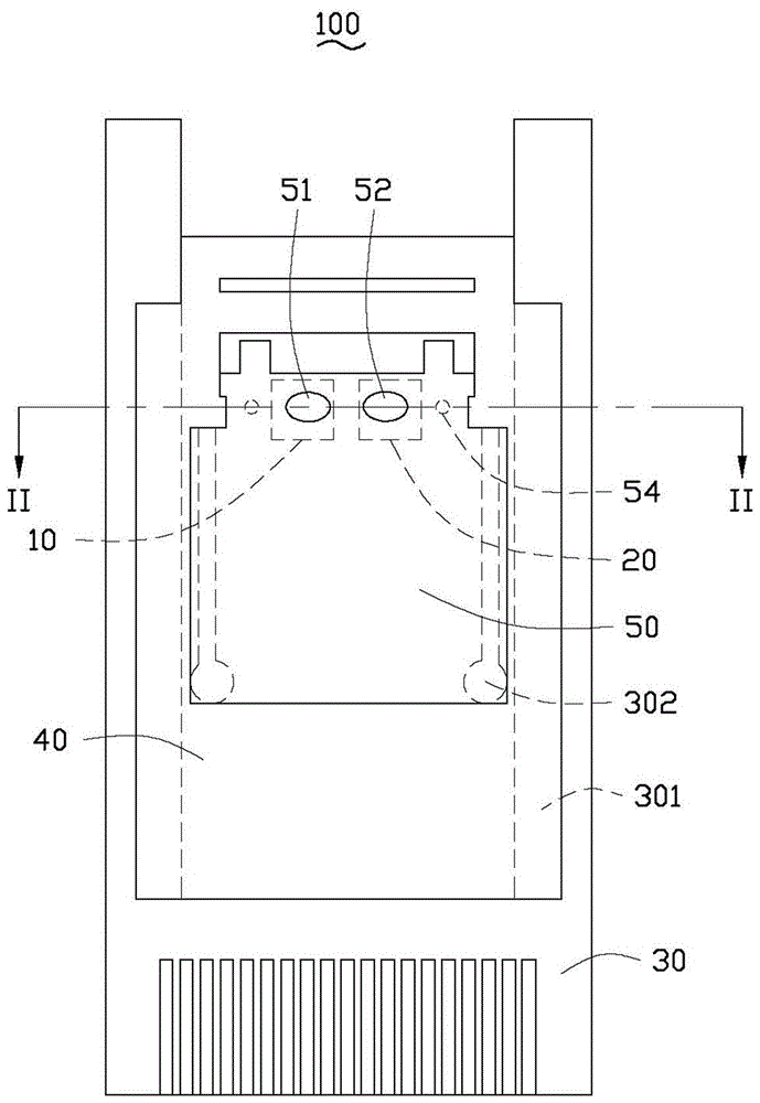
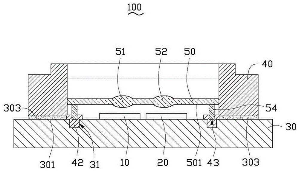
[0011] see figure 1 and figure 2 , is a photoelectric conversion device 100 provided in an embodiment of the present invention, which includes a light emitting module 10 , a light receiving module 20 , a circuit board 30 , a positioning frame 40 and an optical coupling lens 50 .
[0012] The light emitting module 10 and the light receiving module 20 are disposed on the circuit board 30 and electrically connected to the circuit board 30 .
[0013] The circuit board 30 is provided with two first positioning members 31 , and is provided with two first glue-coated areas 301 and two second glue-coated areas 302 . Glue 303 is disposed on the first glue area 301 and the second glue area 302 . The quantity of the first glued area 301 and the second glued area 302 is not limited to this embodiment.
[0014] The positioning frame 40 includes two second positioning members 42 . The two second positioning members 42 correspond to the two first positioning members 31 one by one, and c...
PUM
 Abstract
Description
Claims
Application Information