Single-layer multi-point type touch conducting film and single-layer multi-point type touch screen

A single-layer multi-point, conductive film technology, applied in the direction of electrical digital data processing, instruments, data processing input/output process, etc., can solve the problems of pollution, waste of precious metals, high cost, etc., to simplify the process and reduce alignment Requirements, cost reduction effect

Inactive Publication Date: 2013-12-04
NANCHANG O FILM TECH CO LTD +2
View PDF4 Cites 6 Cited by
  • Summary
  • Abstract
  • Description
  • Claims
  • Application Information

AI Technical Summary

Problems solved by technology

Although the manufacturing technology of the touch screen is developing rapidly, taking the projected capacitive screen as an example, the basic manufacturing process of the ITO layer has not changed much in recent years. It is always inevitable to need ITO coating and ITO patterning.
[0003] Indium is an expensive metal material, so using ITO as the material of the conductive layer greatly increases the cost of the touch screen
Furthermore, in the patterning process of the ITO conductive layer, the entire plated ITO film needs to be etched to form an ITO pattern. In this process, a large amount of ITO is etched away, resulting in a large amount of precious metal waste and pollution.
[0004] Therefore, the ITO material and the corresponding process make the product cost high, resulting in a high cost of the traditional single-layer multi-touch conductive film

Method used

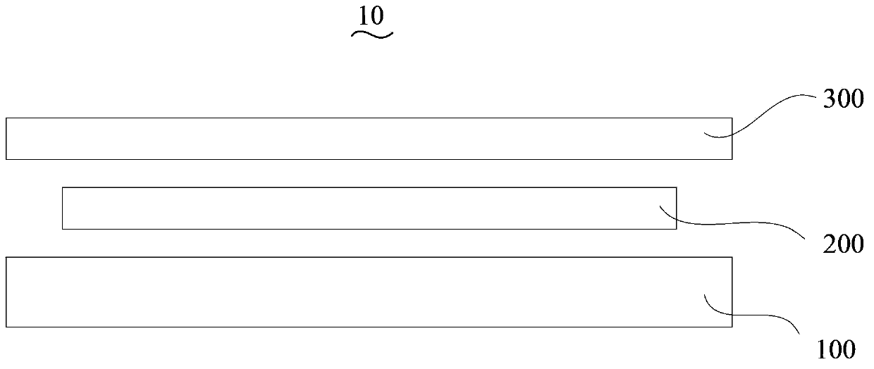
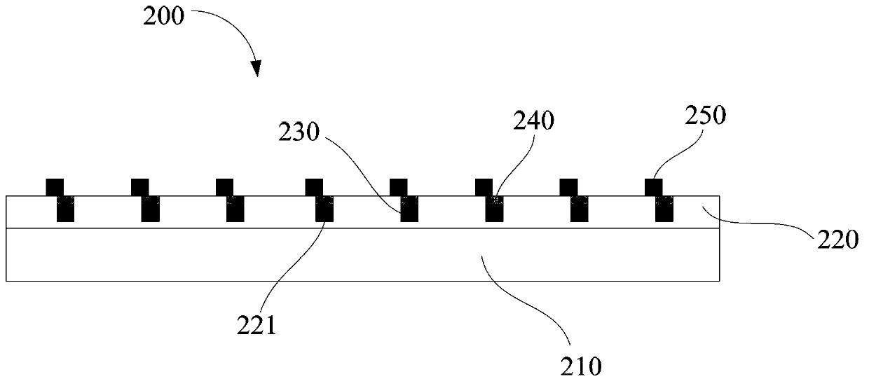
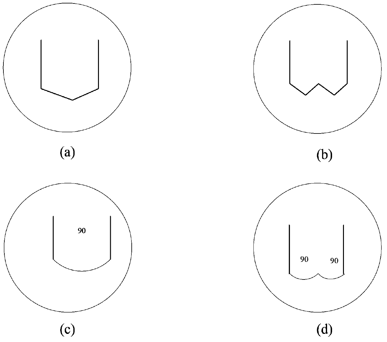

Image

  • Single-layer multi-point type touch conducting film and single-layer multi-point type touch screen
  • Single-layer multi-point type touch conducting film and single-layer multi-point type touch screen
  • Single-layer multi-point type touch conducting film and single-layer multi-point type touch screen

Examples


Embodiment Construction

[0040] In order to facilitate the understanding of the present invention, the present invention will be described more fully below with reference to the associated drawings. Preferred embodiments of the invention are shown in the accompanying drawings. However, the present invention can be embodied in many different forms and is not limited to the embodiments described herein. On the contrary, these embodiments are provided to make the understanding of the disclosure of the present invention more thorough and comprehensive.

[0041] It should be noted that when an element is referred to as being “fixed” to another element, it can be directly on the other element or there can also be an intervening element. When an element is referred to as being "connected to" another element, it can be directly connected to the other element or intervening elements may also be present. The terms "vertical," "horizontal," "left," "right," and similar expressions are used herein for purposes ...


PUM


Abstract

The invention provides a single-layer multi-point type touch conducting film, and further provides a single-layer multi-point type touch screen. The single-layer multi-point type touch conducting film comprises a transparent substrate, a first conducting layer, an insulating layer and a second conducting layer, wherein the transparent substrate comprises a sensing region and a frame region adjacent to the sensing region; the first conducting layer is of a grid shape, is arranged in the sensing region of the transparent substrate, and comprises crossed first conductive threads, the sensing region is provided with a grid groove, and the first conducting layer is accommodated in the grid groove; the insulating layer is located above the first conductive threads and is embedded into the grid groove; the second conducting layer is of a grid shape, is arranged in the sensing region of the transparent substrate, is separated from the first conducting layer through the insulating layer, and comprises crossed second conductive threads, grids of the first conducting layer or grids of the second conducting layer are regular grids, and grids of the other layer are random grids. The single-layer multi-point type touch conducting film is low in cost.

Description

【Technical field】 [0001] The invention relates to a touch conductive film, in particular to a single-layer multi-point touch conductive film and a single-layer multi-point touch screen using the single-layer multi-point touch conductive film. 【Background technique】 [0002] The transparent conductive film is the sensing element in the touch screen that receives input signals such as touch. Currently, the ITO (Indium Tin Oxide) layer is a vital component in transparent conductive films. Although the manufacturing technology of touch screen is developing rapidly, taking the projected capacitive screen as an example, the basic manufacturing process of the ITO layer has not changed much in recent years, and ITO coating and ITO patterning are always unavoidable. [0003] Indium is an expensive metal material, so using ITO as the material of the conductive layer greatly increases the cost of the touch screen. Furthermore, in the patterning process of the ITO conductive layer, th...

Claims


Application Information

Patent Timeline
Patent Type & Authority Applications(China)
IPC IPC(8): G06F3/041G06F3/044
Inventor 杨广舟孙超
Owner NANCHANG O FILM TECH CO LTD
Why Eureka
Try Eureka