Data reading and writing method and device for flash memory equipment and host system

A flash memory storage, host system technology, applied in memory systems, electrical digital data processing, memory address/allocation/relocation, etc., can solve the problem of low data read and write efficiency, reduce copying, and improve read and write efficiency.

Active Publication Date: 2013-12-04
SHENZHEN NETCOM ELECTRONICS CO LTD
View PDF5 Cites 38 Cited by
  • Summary
  • Abstract
  • Description
  • Claims
  • Application Information

AI Technical Summary

Problems solved by technology

[0003] The purpose of the embodiments of the present invention is to provide a method for reading and writing data of a flash memory storage device, so as to solve the problem of low data read and write efficiency caused by address misalignment in existing flash memory storage devices

Method used


Image

  • Data reading and writing method and device for flash memory equipment and host system
  • Data reading and writing method and device for flash memory equipment and host system
  • Data reading and writing method and device for flash memory equipment and host system

Examples


Embodiment 1

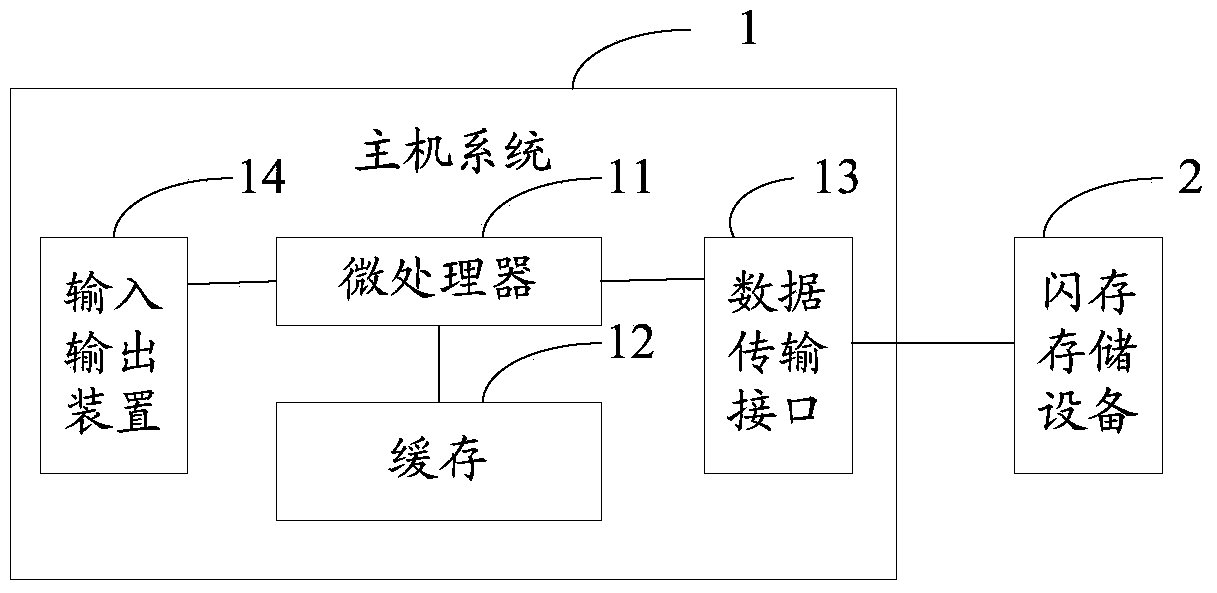
[0037] figure 1 A system scenario to which the method for reading and writing data of a flash memory storage device provided in Embodiment 1 of the present invention is applicable is shown. For convenience of description, only parts related to this embodiment are shown.

[0038] Such as figure 1 As shown, the system includes a host system 1 and a flash storage device 2 .

[0039] Wherein, the host system 1 includes a microprocessor 11 , a cache 12 , a data transmission interface 13 and an input or output device 14 .

[0040] The host system 1 is connected to the flash storage device 2 through the data transmission interface 13 . The user sends a write command to the microprocessor 11 through the input / output device 14, and the microprocessor 11 sends the write command to the flash storage device 2 through the data transmission interface 13, and the write command includes the The data in the cache 12 and the address where the data is written into the flash storage device 2 ....

Embodiment 2

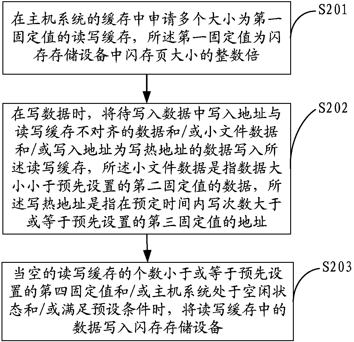
[0070] figure 2 The implementation flow of the method for reading and writing data of a flash memory storage device provided by Embodiment 2 of the present invention is shown, and the process of the method is described in detail as follows:

[0071] In step S201, a plurality of read-write caches with a size of a first fixed value are applied for in the cache of the host system, and the first fixed value is an integer multiple of the size of a flash memory page in the flash storage device.

[0072] In this embodiment, the cache of the host system is divided into multiple read-write caches according to a preset first fixed value. Optionally, it is also possible to select a part (according to a preset ratio, such as 50%) of the divided read-write caches from the plurality of read-write caches for caching writes to the flash memory storage device and / or from the flash memory storage device. The read data; in addition, it is also possible to select part of the cache of the host s...

Embodiment 3

[0140] Figure 12 The implementation flow of the method for reading and writing data of a flash memory storage device provided by Embodiment 3 of the present invention is shown, and the process of the method is described in detail as follows:

[0141] In step S1201, multiple read-write caches with a size of a first fixed value are applied for in the cache of the host system, and the first fixed value is an integer multiple of the size of a flash memory page in the flash storage device.

[0142] This step is the same as step S201 in the second embodiment, and the specific implementation process is as described in step S201 in the second embodiment, and will not be repeated here.

[0143] In step S1202, the data whose read address is the read hot address or the data on the address continuous with the current read address is read from the flash storage device into the read-write cache in advance, wherein the read hot address is The address currently having data read;

[0144] I...


PUM


Abstract

The invention is suitable for the technical field of data storage, and provides a data reading and writing method and device for flash memory equipment and a host system. The method comprises the following steps: applying for a plurality of reading and writing caches of first fixed values in the cache of the host system, wherein the first fixed values are integer times of flash memory pages in the flash memory equipment; during data writing, writing data of which the writing address are unaligned with the reading and writing caches and / or small file data and / or data of which the writing addresses are writing hot addresses in data to be written into the reading and writing caches; and when the number of empty reading and writing caches is smaller than or equal to a preset fourth fixed value and / or the host system is in an idle state and / or satisfies a preset condition, writing data in the reading and writing caches into the flash memory equipment. according to the method, the device and the system, the problems of data copy and migration performed continuously in a writing process due to misalignment of addresses or writing of the small file data can be reduced greatly, and the data reading and writing efficiency of the flash memory equipment is increased.

Description

technical field [0001] The invention belongs to the technical field of data storage, and in particular relates to a method, a device and a host system for reading and writing data of a flash memory storage device. Background technique [0002] The data read and write speed of flash memory storage devices is an important aspect to measure the performance of flash memory storage devices. However, when the existing flash memory storage device writes data whose address is not aligned (meaning that the address is not an integer multiple of the machine word length), it needs to continuously copy and move data, which limits the flash memory storage device to a certain extent. Further improvements in read and write speeds. Although the existing technology can align addresses by adding a page offset, this method needs to calculate the offset of the flash storage device page in advance, and the operation is more complicated and the efficiency is lower. Moreover, since the conditions...

Claims


Application Information

Patent Timeline
Patent Type & Authority Applications(China)
IPC IPC(8): G06F12/08G06F12/0893
Inventor 豆威
Owner SHENZHEN NETCOM ELECTRONICS CO LTD
Why Eureka
Try Eureka